Advancements in Telecom PCB Assembly for Enhanced Connectivity
Key Takeaways
The landscape of telecom PCB assembly has witnessed substantial progress, reflecting the continuous demand for high-performance communication systems. One of the primary shifts in this sector is the advent of innovative materials in PCB design, which enhance signal integrity and reduce loss. These advanced materials not only improve durability but also support higher frequencies, which is vital for modern telecommunication needs.
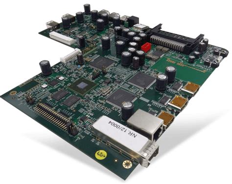
Furthermore, efficient manufacturing techniques are essential in transforming PCB assembly processes. Techniques such as surface mount technology (SMT) have optimized production lines, allowing for faster assembly and reduced costs. As demand intensifies for smaller and more complex devices, the impact of miniaturization becomes increasingly significant. Miniaturized PCBs are pivotal in enabling compact designs that still deliver robust performance.
Moreover, automation plays a crucial role in enhancing production efficiency and accuracy during PCB assembly. The integration of robotics and AI-driven systems minimizes human error and accelerates manufacturing cycles, ultimately driving down turnaround times. With the future leaning towards more connectivity solutions, evolving trends in telecom PCB technology promise even greater capabilities.
In summary, the continuous evolution within telecom PCB assembly not only meets current industry demands but also shapes future communication technologies, ensuring an interconnected world that thrives on innovative solutions. Below is a summary table highlighting key advancements:
| Advancements | Description |
|---|---|
| Innovative Materials | Enhance signal integrity and reduce loss |
| Efficient Manufacturing Techniques | Faster assembly with reduced costs |
| Automation | Minimizes human error and accelerates production cycles |
| Miniaturization | Enables compact designs while maintaining robust performance |
Emphasizing these trends solidifies the role of PCB assembly in enhancing connectivity across various platforms and services fundamental to modern telecommunications.
The Evolution of Telecom PCB Assembly: A Historical Perspective
The landscape of telecom PCB assembly has undergone significant transformations over the decades. Initially, the process was rudimentary, relying on basic techniques and materials that limited functionality and efficiency. However, the rapid advancement in telecommunication technology necessitated a shift towards more sophisticated pcb assembly methods. In the early days, traditional materials dominated the industry, but as demand for faster and more reliable connectivity grew, innovative materials began to emerge. Today, telecommunications relies heavily on PCBA (Printed Circuit Board Assembly) techniques that incorporate advanced components and multi-layered boards to enhance performance.
With the rise of mobile communication in the late 20th century, there was an urgent need for higher-density designs—a challenge met by advancements in pcb assembly that enabled miniaturization and increased circuit complexity without compromising quality. The introduction of surface mount technology (SMT) transformed traditional methods by allowing components to be mounted directly onto the surface of PCBs with greater precision. This change not only accelerated manufacturing processes but also improved electrical performance significantly.
"Embracing new technologies in telecom PCB assembly not only optimizes production but also meets ever-evolving consumer demands for connectivity."
As we look back at this evolution, it’s clear that each breakthrough has played a pivotal role in shaping a more connected world. The improvements in manufacturing efficiency have paved the way for innovative solutions that cater to a variety of applications—from consumer electronics to critical infrastructure systems—underscoring telecom’s vital role in modern society’s communication framework. Through continuous adaptation and advancement, pcb assembly remains at the forefront of technological progress within telecommunications.
Innovative Materials in Telecom PCB Design
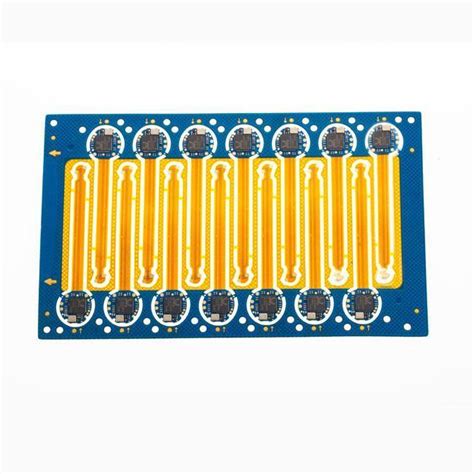
The field of telecom PCB assembly is witnessing a remarkable transformation driven by the introduction of innovative materials that enhance the performance and durability of printed circuit boards (PCBs). These advancements are crucial as they address the growing demands for higher frequencies, improved thermal management, and increased miniaturization in communication devices. The use of materials such as high-frequency laminates, which possess excellent dielectric properties, allows for enhanced signal integrity and performance in high-speed applications. Additionally, ceramic-based substrates are gaining popularity due to their superior thermal properties, which are essential for managing heat in densely packed assemblies. The integration of flexible PCBs also plays a pivotal role, enabling designers to innovate in form factors and layout design while ensuring reliability. Moreover, advancements in environmentally friendly materials are paving the way for sustainable practices within PCB assembly, allowing manufacturers to reduce their ecological footprint without compromising on quality. As telecom technologies evolve, these cutting-edge materials not only enhance the functionality of telecom products but also redefine how connectivity solutions are engineered, setting a strong foundation for future developments in the sector.
Efficient Manufacturing Techniques Transforming PCB Assembly
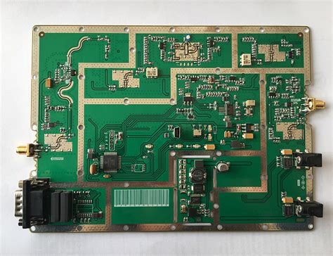
As the demand for high-performance telecom products surges, efficient manufacturing techniques in pcb assembly are becoming pivotal in driving advancements within the industry. The integration of cutting-edge methods, such as automated assembly, is revolutionizing traditional pcba processes, allowing for faster production cycles and reduced human error. Techniques like Surface Mount Technology (SMT) and Through-Hole Technology (THT) have been optimized to maximize production efficiency while maintaining high quality and reliability in pcb assembly. Moreover, the application of smart manufacturing concepts, including real-time monitoring and adaptive process control, enhances operational efficiency by identifying bottlenecks early in the production line. Additionally, the use of advanced materials tailored for specific applications provides improved electrical performance and thermal management, crucial for telecom devices that require consistent connectivity. These innovations not only reduce costs but also enable manufacturers to meet the strict timelines demanded by the rapidly evolving telecom sector. Consequently, the synergy of these modern techniques underpins a transformative shift in pcb assembly, driving forward the evolution of communication technologies and reinforcing enhanced connectivity across networks.
The Role of Automation in Enhancing PCB Production
Automation plays a pivotal role in the realm of pcb assembly, significantly improving efficiency and quality within the production process. As the demand for high-performance electronics continues to escalate, particularly in telecommunications, the integration of advanced automated systems has become essential. By employing robotic technologies and sophisticated software, industries can streamline pcba processes, reducing human error and enhancing precision. Automated inspection systems further ensure that each pcb assembly meets rigorous quality standards, providing a reliable foundation for telecom devices that require utmost connectivity. Moreover, these innovations enable quicker turnaround times, allowing companies to respond swiftly to market demands and technological advancements. The shift towards automation not only elevates production capabilities but also facilitates the use of cutting-edge materials in pcb assembly, ultimately shaping the future of communication technology and its myriad applications. In this evolving landscape, it is evident that automation is not just an enhancement; it is a fundamental driver in optimizing pcba for enhanced connectivity solutions across various sectors.
Impact of Miniaturization on Telecom Connectivity Solutions
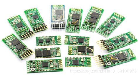
The trend of miniaturization in telecom PCB assembly has led to significant advancements in connectivity solutions, influencing everything from device design to operational efficiency. As consumer demand for smaller, lighter, and more powerful devices continues to rise, the importance of PCBA becomes evident, as it allows for the integration of high-density components without compromising performance. This shift towards miniaturization fosters innovative materials and refined manufacturing techniques that are pivotal in creating compact yet robust designs. The utilization of advanced substrates coupled with more efficient electronic layouts enables manufacturers to produce smaller boards without sacrificing power or functionality. Additionally, this transformation helps reduce weight and energy consumption, which is critical in mobile and portable telecom solutions. As communication technology evolves, embracing the miniaturization trend not only enhances product performance but also optimizes manufacturing processes, ultimately leading to better connectivity outcomes across various platforms. The evolution toward compactness is reshaping how telecom industries approach product development and consumer engagement in an increasingly connected world.
Future Trends in Telecom PCB Technology
As the telecommunications sector continues to evolve, the future of PCB assembly holds significant promise with emerging trends that prioritize efficiency, connectivity, and advanced technology integration. One of the key directions for PCBA development is the shift towards high-frequency applications that demand precision. Manufacturers are increasingly leveraging advanced materials that facilitate improved signal integrity while minimizing losses. This is leading to more compact designs that still support high data rates essential for modern communication systems.
Moreover, the trend towards integrated circuits in PCB design allows for a streamlined approach where multiple functions can be combined onto a single board, thus enhancing overall performance and reducing space requirements. The fusion of automation in production processes also plays a pivotal role; automated systems enhance precision in pcb assembly, thus driving down costs while maintaining consistent quality — a vital aspect as telecom networks expand globally.
Additionally, with the growing emphasis on eco-friendly practices, sustainable materials are becoming more prevalent in PCB manufacturing. These innovations not only appeal to regulatory standards but also align with consumer demand for green technology solutions. It is clear that as we look forward, the interplay between innovative materials, efficient manufacturing techniques, and automation will set the trajectory for telecom pcb assembly, enabling enhanced connectivity on a global scale.
Sustainable Practices in PCB Manufacturing for Telecommunications
In the pursuit of more responsible and environmentally friendly practices, the telecommunications industry is increasingly focused on sustainable practices in PCB manufacturing. The integration of materials that are either recyclable or biodegradable is becoming common in pcb assembly processes. By utilizing eco-friendly materials, manufacturers minimize waste and reduce the carbon footprint associated with production. Additionally, employing energy-efficient manufacturing techniques not only lowers operational costs but also contributes to a significant decrease in environmental impact. The use of water-based adhesives and eco-conscious soldering techniques further enhances the sustainability of PCBA processes. As the industry evolves, a concerted effort to implement green technologies will not only meet regulatory compliance but will also resonate with environmentally aware consumers, fostering a market shift towards sustainability. Moreover, innovations such as closed-loop recycling systems allow manufacturers to reclaim materials from old boards, ensuring that valuable resources are reused. This commitment to sustainability reflects the broader goal of enhancing connectivity while respecting our planet’s resources and paving the way for a more sustainable future in telecommunications.
Challenges and Solutions in Modern Telecom PCB Assembly
The field of pcb assembly for telecommunications faces a myriad of challenges, primarily due to the rapid evolution of technology and the increasing demand for higher performance and smaller devices. One significant challenge is ensuring signal integrity in densely packed pcba, where the proximity of traces can lead to interference and crosstalk. To mitigate these issues, engineers are now employing advanced design techniques such as controlled impedance routing and careful layer stack management, which enhance performance while adhering to stringent size constraints.
Another critical hurdle is the integration of innovative materials that can withstand the rigors of modern telecommunications. Traditional materials may not meet the thermal or electrical demands posed by next-generation communications, necessitating the adoption of new composites. Solutions like halogen-free laminates and ultra-thin substrates are gaining traction in pcb assembly processes to enhance durability and reliability.
Additionally, managing production costs while ensuring high quality remains a constant struggle. Implementing lean manufacturing principles allows companies to optimize their processes, reduce waste, and maintain strict quality control during the pcba production stages. By leveraging automation and real-time data analytics, operations can be streamlined while minimizing human error. This holistic approach not only addresses immediate challenges but also lays a foundation for sustainable growth within the telecom sector as demand for connectivity continues to escalate.
Conclusion
In conclusion, the realm of telecom PCB assembly has undergone significant transformation, marked by an array of advancements that are reshaping the industry and driving enhanced connectivity. The intricate design of PCBA is now complemented by the use of advanced materials and innovative techniques that facilitate more efficient manufacturing processes. As we have explored, the integration of automation plays a pivotal role in optimizing production, allowing manufacturers to achieve higher precision and reduced assembly times. Furthermore, the ongoing push towards miniaturization not only enhances the performance of communication devices but also streamlines connectivity solutions. Looking ahead, sustainable practices are becoming increasingly crucial in PCB assembly, ensuring that environmental considerations are addressed without compromising performance and reliability. By embracing these advancements and adapting to emerging trends, stakeholders in the telecom sector can expect to foster further innovations in communication technology, ultimately paving the way for a more connected world.
FAQs
What is PCB assembly in the context of telecommunications?
PCB assembly, commonly referred to as PCBA, involves the process of soldering electronic components onto a printed circuit board (PCB) to create a functional circuit that supports communication technologies. This process is crucial for ensuring reliable connectivity in telecom applications.
What advancements have been made in PCB assembly for telecom applications?
Recent advancements include the use of innovative materials, improved methodologies, and automation that streamline the pcb assembly process, enhancing efficiency, accuracy, and overall performance in telecommunication devices.
How does automation affect PCB assembly?
Automation significantly reduces production times and minimizes human error in the pcb assembly process. With robotic systems and smart manufacturing techniques, companies can achieve greater consistency and higher output levels.
Why is miniaturization important in telecom PCB designs?
Miniaturization leads to smaller, lighter devices that can handle higher data rates while consuming less space. This is essential for modern telecommunications where compactness and efficiency are vital.
What are some sustainable practices in PCB manufacturing?
Sustainable practices include using eco-friendly materials, reducing waste during production processes, and recycling old components. These initiatives not only benefit the environment but also contribute to more efficient pcba processes.
What challenges do manufacturers face in modern PCB assembly?
Manufacturers often encounter challenges such as complexity in design requirements, maintaining quality control during high-volume production, and keeping pace with rapid technological advancements while still adhering to regulatory standards.


