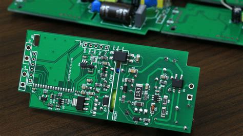
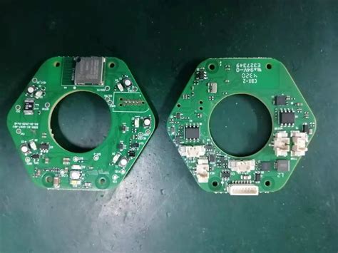
Advantages of multilayer pcb
Multilayer printed circuit boards (PCBs) play a crucial role in modern electronic devices, and their high-density wiring advantages are particularly significant.
First, multi-layer PCBs can accommodate more circuits and components in a limited space, which is crucial for today’s electronic products that pursue miniaturization and high performance.
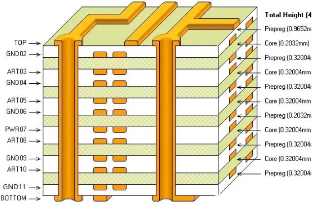
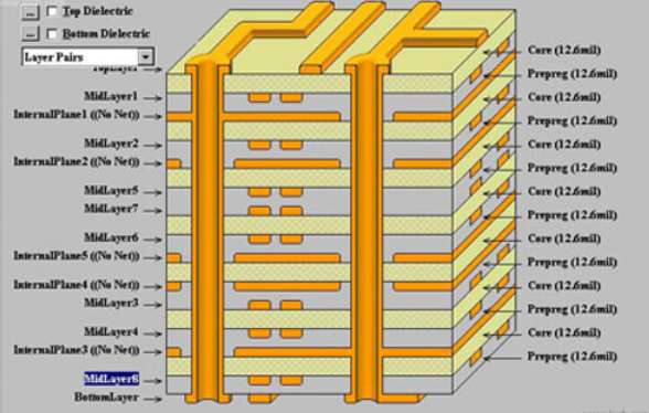
By increasing the number of layers, designers can distribute signal lines, power lines, and ground lines between different layers, thereby effectively reducing signal interference and electromagnetic interference.
This design not only improves the stability and reliability of the circuit, but also makes the implementation of complex circuits possible.
In addition, the high-density wiring of multi-layer PCBs significantly improves circuit performance. Since multi-layer PCBs can transmit signals between different layers, the signal path is shortened, thereby reducing signal delays and losses.
This is particularly important for high-speed signal transmission, especially in communication equipment and computer systems, where signal integrity and transmission speed directly affect the overall performance of the equipment.
By optimizing the wiring path, multi-layer PCB can ensure fast and accurate transmission of signals to meet the needs of high-performance electronic equipment.
At the same time, the high-density wiring of multi-layer PCBs also brings greater design flexibility. Designers can freely distribute circuits between different layers, avoiding the problem of insufficient wiring space in single-layer or double-layer PCBs.
This flexibility allows designers to better optimize circuit layout and improve circuit integration and functionality. For example, in complex embedded systems, multi-layer PCBs can tightly integrate processors, memories and other key components to achieve higher system integration and stronger functionality.
In addition, the high-density wiring of multi-layer PCBs also significantly improves the heat dissipation performance of the circuit. Because multi-layer PCBs can distribute power and ground lines between different layers, an effective heat dissipation channel is formed to help electronic components dissipate heat better.
This is particularly important for high-power electronic equipment, which can effectively extend the service life of the equipment and improve its reliability and stability.
To sum up, the high-density wiring advantages of multi-layer PCB play an irreplaceable role in modern electronic equipment. By improving the integration, performance and design flexibility of the circuit, multi-layer PCB not only meets the needs of miniaturization and high performance, but also significantly improves the stability and reliability of the circuit. With the continuous development of electronic technology, multi-layer PCB will continue to play an important role in future electronic product design, providing a solid foundation for achieving more efficient and reliable electronic equipment.
Multilayer PCB in signal integrity Advantages in aspects
Multilayer printed circuit boards (PCBs) play a vital role in modern electronic equipment, and their advantages in signal integrity are particularly significant.
First of all, multi-layer PCB can effectively reduce the length of the signal path by increasing the number of layers,
thereby reducing delay and loss in signal transmission. This design allows signals to be transmitted faster and more accurately, greatly improving the performance and reliability of the device.
In addition, the structural design of multi-layer PCB helps reduce electromagnetic interference (EMI).
In a multi-layer PCB, the signal layer and the ground layer can be tightly coupled. This tight coupling can form an effective shielding layer to reduce the impact of external electromagnetic interference on the signal. At the same time, the shielding effect between internal layers can also prevent mutual interference between signals, thereby ensuring signal integrity and stability.
Furthermore, multi-layer PCBs can also provide better power distribution.
By distributing power and ground between different layers, power and ground noise can be effectively reduced. This design can not only improve the stability of the power supply, but also reduce the interference of power supply noise on the signal, ensuring the clarity and accuracy of signal transmission.
It is worth mentioning that multi-layer PCB performs particularly well in high-frequency signal transmission.
High-frequency signals have very strict requirements on the transmission path, and any small interference may cause signal distortion.
By optimizing the inter-layer structure and material selection, multi-layer PCB can provide a low-loss, high-fidelity signal transmission path to meet the strict requirements of high-frequency signal transmission.
In addition, the design of multi-layer PCB can also increase the density and integration of circuits.
By increasing the number of layers, more circuit components can be arranged in a limited space, allowing for more complex circuit designs. This high-density design not only saves space, but also improves the overall performance and functionality of the circuit.
In short, the superiority of multi-layer PCB in signal integrity is reflected in many aspects.
By reducing signal path length, reducing electromagnetic interference, optimizing power distribution, improving high-frequency signal transmission performance, and increasing circuit density, multilayer PCBs provide reliable and efficient solutions for modern electronic devices.
These advantages have made multi-layer PCB widely used in the electronics industry and become an important force in promoting technological progress.
Application of multi-layer PCB in electromagnetic interference control
Multilayer printed circuit boards (PCBs) play a vital role in modern electronic devices, especially in electromagnetic interference (EMI) control.
First of all, multi-layer PCB effectively reduces the generation and spread of electromagnetic interference through its unique structural design.
Because multilayer PCBs can place power and ground layers closely together, this design can form a low-impedance power distribution network, thereby reducing power supply noise and electromagnetic radiation.
In addition, the interlayer shielding effect of multi-layer PCB also significantly reduces the impact of electromagnetic interference.
By inserting a ground layer or power layer between signal layers, multi-layer PCBs can effectively shield electromagnetic interference and protect sensitive signals from external interference.
Furthermore, multi-layer PCBs also perform well in terms of signal integrity.
Since multi-layer PCBs can provide shorter signal paths and better impedance matching, this helps reduce signal reflections and crosstalk, thereby improving the quality and reliability of signal transmission.
Especially in high-speed circuit design, the advantages of multi-layer PCB are more obvious. Through reasonable stacking design and wiring strategy, multi-layer PCB can ensure the integrity of high-speed signals and reduce signal distortion and delay.
In addition, multi-layer PCBs also have significant advantages in thermal management.
Electronic equipment generates a large amount of heat during operation. If the heat cannot be effectively dissipated, the performance of the equipment may be reduced or even damaged.
Through its multi-layer structure, multi-layer PCB can better disperse and conduct heat, thereby improving the heat dissipation efficiency of the device. This not only extends the service life of the equipment, but also improves its reliability and stability.
It is worth mentioning that multi-layer PCB also has higher design flexibility. Since multi-layer PCBs can accommodate more wiring layers, designers have more choices and space when designing complex circuits. Whether it is high-density component layout or complex circuit connections, multi-layer PCB can provide better solutions. This design flexibility not only improves the efficiency of circuit design, but also enables electronic devices to achieve more functions and higher performance.
To sum up, multi-layer PCBs perform well in aspects such as electromagnetic interference control, signal integrity, thermal management and design flexibility. Its unique structural design and superior performance make it an indispensable and important part of modern electronic equipment. By rationally utilizing the advantages of multi-layer PCBs, electronic devices can achieve higher performance, better reliability and longer service life, thereby meeting the evolving technical needs and market demands.
More Importance of Layer PCB in Miniaturized Electronic Devices
Multilayer printed circuit boards (PCBs) play a vital role in modern miniaturized electronic devices. With the continuous advancement of technology, electronic devices are becoming more and more powerful while becoming smaller and smaller. This trend has put forward higher requirements for the design and manufacturing of circuit boards. Multilayer PCB successfully meets these needs through its unique structure and advantages.
First of all, multi-layer PCB can significantly increase the density of circuits.
Compared with single-layer or double-layer PCB, multi-layer PCB can accommodate more circuits and components in a limited space.
This high-density circuit design allows electronic devices to integrate more functions without increasing the size. For example, miniaturized electronic products such as smartphones, tablets, and wearable devices rely on the high-density characteristics of multi-layer PCBs to achieve their complex functions and compact designs.
Secondly, multi-layer PCB has significant advantages in signal transmission.
Since multi-layer PCB can distribute and isolate signals between different layers, it can effectively reduce signal interference and crosstalk problems.
This is especially important for high-speed signal transmission, where any tiny interference may cause signal distortion or data loss.
By using multi-layer PCBs, designers can better control the signal path, ensuring signal integrity and stability.
In addition, multi-layer PCBs also have better heat dissipation performance. In miniaturized electronic devices, heat dissipation has always been an important challenge.
Through its multi-layer structure, multi-layer PCB can disperse and conduct heat more effectively and avoid local overheating. This not only helps extend the life of electronic equipment, but also improves its efficiency and reliability.
Furthermore, multi-layer PCBs also excel in design flexibility. Multi-layer structures allow designers to perform complex circuit layouts and connections between different layers, allowing for greater design freedom.
This flexibility enables multi-layer PCBs to adapt to various complex circuit design needs and meet the functional requirements of different electronic devices.
Finally, multi-layer PCBs also have certain advantages in terms of production cost and time. Although the initial design and manufacturing costs of multi-layer PCBs are higher, their high density and high performance characteristics can reduce the number of components and wiring complexity, thereby reducing overall production costs and time.
In addition, with the continuous advancement of multi-layer PCB manufacturing technology, its production efficiency and quality are also constantly improving, making multi-layer PCB an ideal choice for miniaturized electronic devices.
To sum up, the importance of multi-layer PCB in miniaturized electronic devices is self-evident. Its high density, high performance, good heat dissipation performance and design flexibility make multilayer PCB an indispensable part of modern electronic equipment. With the continuous development of technology, multi-layer PCB will play a more important role in future electronic devices.
Thermal management and heat dissipation performance analysis of multi-layer PCB
Multilayer printed circuit boards (PCBs) play a crucial role in modern electronic devices, and their thermal management and heat dissipation properties are particularly outstanding.
First of all, multi-layer PCB effectively improves thermal management capabilities through its unique structural design.
Multilayer PCBs are usually made up of multiple layers of conductive materials and insulating materials alternately stacked. This structure not only increases the density of the circuit, but also provides more heat conduction paths. By distributing the heat source between different layers, heat can be dispersed more evenly, thus avoiding the hot spot problem common in single-layer PCBs.
In addition, the heat dissipation performance of multi-layer PCBs has been significantly improved.
Because multi-layer PCBs can embed thermally conductive materials, such as copper foil or thermally conductive fillers, between different layers, these materials have excellent thermal conductivity and can quickly conduct heat from high-temperature areas to low-temperature areas.
This results in a more even temperature distribution across the board, reducing the risk of local overheating.
At the same time, multi-layer PCBs can further enhance the heat dissipation effect by adding designs such as heat dissipation vias and heat dissipation pads.
These designs not only improve heat conduction efficiency, but also increase the heat dissipation area, thereby effectively reducing the overall temperature of the circuit board.
It is worth mentioning that the thermal management and heat dissipation performance of multi-layer PCBs are particularly important in high-power electronic equipment.
As the power of electronic devices continues to increase, thermal management has become a key design challenge.
Multi-layer PCB can effectively meet this challenge through its superior thermal management and heat dissipation performance, ensuring that the device can still maintain stable working status when operating at high power.
For example, in high-frequency communication equipment and high-power LED lighting systems, the application of multi-layer PCBs significantly improves the reliability and service life of the equipment.’As the power of electronic devices continues to increase, thermal management has become a key design challenge.
Multi-layer PCB can effectively meet this challenge through its superior thermal management and heat dissipation performance, ensuring that the device can still maintain stable working status when operating at high power.
For example, in high-frequency communication equipment and high-power LED lighting systems, the application of multi-layer PCBs significantly improves the reliability and service life of the equipment.
In addition, the thermal management and heat dissipation performance of multi-layer PCBs also play a positive role in promoting the miniaturization and high-density integration of electronic devices.
As electronic devices develop towards miniaturization and high-density integration, the thermal management and heat dissipation issues of circuit boards have become more complex.
Through its multi-layer structure and efficient thermal management design, multi-layer PCB can achieve efficient heat dissipation in a limited space, thereby supporting higher density component integration.
This not only improves the performance of the circuit board, but also provides the possibility for miniaturization of electronic equipment.
In summary, multi-layer PCBs have significant advantages in thermal management and heat dissipation performance. Through its unique structural design and efficient heat conduction materials, it can effectively disperse heat, avoid hot spot problems, and perform well in high-power electronic equipment. At the same time, the superior performance of multi-layer PCB also provides strong support for the miniaturization and high-density integration of electronic equipment. Therefore, multi-layer PCB has broad application prospects in modern electronic equipment and has important technical and market value.