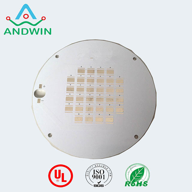
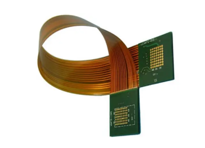
All flex pcb
Manufacturing process and technology of fully flexible PCB
The manufacturing process and technology of fully flexible PCB (Printed Circuit Board) occupies an important position in the field of modern electronic manufacturing. With the increasing miniaturization and complexity of electronic equipment, fully flexible PCB has become the first choice for many high-tech products due to its unique flexibility and lightweight characteristics. However, to achieve high-quality fully flexible PCB, the refinement and specialization of manufacturing process and technology are essential.
First of all, the selection of manufacturing materials for fully flexible PCB is crucial. Generally, polyimide (PI) and polyester (PET) are the most commonly used substrates. These materials not only have excellent electrical properties, but also remain stable in high temperature environments. Selecting a suitable substrate is the first step to ensure the performance of a fully flexible PCB. Next, the selection and treatment of copper foil is also a key link. The thickness and surface treatment of the copper foil directly affect the conductivity and durability of the circuit. A uniform and highly adherent copper layer can be formed on the substrate by electroplating or chemical deposition.
After the material preparation is completed, the graphic transfer process is one of the core steps in manufacturing a fully flexible PCB. Usually, photolithography technology is used to transfer the designed circuit pattern to the copper foil. The precision and stability of photolithography technology directly determine the fineness and reliability of the circuit. Subsequently, the excess copper foil is removed through the etching process, leaving only the required circuit pattern. The etching process requires strict control of time and the concentration of chemical reagents to ensure the integrity and accuracy of the circuit pattern.
In addition, the lamination process of fully flexible PCBs is also an important link. Multi-layer fully flexible PCBs require that multi-layer circuit boards be combined together through lamination technology. During the lamination process, it needs to be carried out under high temperature and high pressure to ensure the close bonding between the layers and the reliability of the electrical connection. The quality of the lamination process directly affects the mechanical and electrical properties of the fully flexible PCB.
Finally, the testing and inspection of fully flexible PCBs are key steps to ensure product quality. After manufacturing is completed, a series of electrical performance tests and mechanical performance tests need to be carried out on the fully flexible PCB. Through these tests, defects that may occur in the manufacturing process can be discovered and corrected to ensure the reliability and stability of the final product.
In summary, the manufacturing process and technology of fully flexible PCBs involve multiple key links, and each link requires refined operation and strict control. By selecting suitable materials, precise graphic transfer, strict etching process, reliable lamination technology, and comprehensive testing and inspection, the high quality and high performance of fully flexible PCBs can be ensured. In the future, with the continuous advancement of technology, fully flexible PCBs will play their unique advantages in more fields and promote the development of the electronics manufacturing industry.
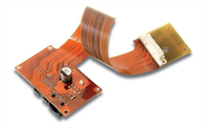
Application of Fully Flexible PCB in Wearable Devices
Fully flexible printed circuit boards (fully flexible PCBs) play an increasingly important role in modern technology, especially in the field of wearable devices. With the advancement of technology and the increasing demand for portability and comfort, fully flexible PCBs have gradually become a key component in the design of wearable devices due to their unique characteristics and broad application prospects.
First of all, the biggest advantage of fully flexible PCBs lies in their excellent flexibility and lightness. Traditional rigid PCBs are often bulky and difficult to adapt to complex three-dimensional structures and dynamic environments. Fully flexible PCBs can be easily bent, folded, and even curled, which allows them to perfectly fit the curves of the human body and provide a more comfortable wearing experience. For example, devices such as smart watches, fitness trackers, and smart glasses can achieve more compact and ergonomic designs through fully flexible PCBs, thereby improving the user experience.
In addition, fully flexible PCBs also have excellent durability and reliability. Wearable devices are often required to be used in various environments, including high temperature, low temperature, humidity, and vibration. Fully flexible PCBs use high-performance polyimide or polyester materials, which can maintain stable performance in extreme environments and are not easy to break or damage. This feature not only extends the service life of the device, but also reduces the frequency of maintenance and replacement, thereby reducing the user’s cost of use.
Furthermore, the high integration and design flexibility of fully flexible PCBs are also one of the reasons why they are popular in wearable devices. Fully flexible PCBs can integrate multiple functional modules, such as sensors, microprocessors, and wireless communication modules, allowing devices to achieve more functions. For example, fully flexible PCBs in smart clothing can integrate functions such as heart rate monitoring, temperature sensing, and GPS positioning to provide users with comprehensive health monitoring and sports data analysis. In addition, the design flexibility of fully flexible PCBs also allows engineers to customize according to specific needs, thereby developing more innovative and differentiated products.
Finally, the application of fully flexible PCBs in wearable devices has also promoted the development of green environmental protection. Traditional electronic products will generate a large amount of electronic waste during the production and disposal process, while fully flexible PCBs significantly reduce the negative impact on the environment due to the recyclability of its materials and low energy consumption during the production process. This not only meets the requirements of modern society for sustainable development, but also establishes a good social responsibility image for enterprises.
In summary, the application of fully flexible PCBs in wearable devices not only improves the comfort and functionality of the equipment, but also enhances its durability and environmental protection. With the continuous advancement of technology and the growth of market demand, fully flexible PCBs will surely play an increasingly important role in the field of wearable devices, promoting continuous innovation and development in this field.
Market Prospects and Development Trends of Fully Flexible PCB
WPAICG_IMAGE
Fully flexible PCB (Printed Circuit Board) is rapidly emerging in the modern electronics industry and has become an important force in promoting technological progress. With the continuous development of science and technology, the demand for lightweight, flexible and high-performance electronic equipment is increasing. With its unique advantages, fully flexible PCB has gradually occupied a place in the market. First of all, the market prospects of fully flexible PCB are broad, mainly due to its wide applicability in a variety of application fields. Whether it is a smartphone, wearable device, or medical device and automotive electronics, fully flexible PCB can provide excellent solutions. Its thin and bendable characteristics enable designers to realize more complex circuit design in a limited space, thereby improving the function and performance of the product.
In addition, the manufacturing process of fully flexible PCB is also constantly improving, which has promoted the growth of its market demand. With the advancement of printed electronics technology and material science, the production cost of fully flexible PCB has gradually decreased, and the production efficiency has been significantly improved. This not only makes fully flexible PCB have an advantage in the high-end market, but also makes it competitive in the mid- and low-end market. At the same time, the increase in environmental awareness has also prompted companies to pay more attention to the sustainability of fully flexible PCB. Compared with traditional rigid PCB, fully flexible PCB produces less waste and lower energy consumption during the production process, which is in line with the concept of green manufacturing.
Looking further, the development trend of fully flexible PCB is also worthy of attention. First of all, with the popularization of 5G technology, the application of fully flexible PCB in communication equipment will be more extensive. 5G equipment has higher performance requirements for circuit boards, and fully flexible PCB can provide higher signal transmission speed and lower signal loss to meet the needs of 5G equipment. Secondly, the rapid development of the Internet of Things (IoT) has also brought new opportunities for fully flexible PCBs. IoT devices usually require miniaturization, lightweight and high reliability, and fully flexible PCBs can meet these requirements and help popularize IoT devices.
In addition, the demand for fully flexible PCBs in the field of medical electronics is also increasing. Modern medical devices are increasingly dependent on high-precision and high-reliability electronic components. Fully flexible PCBs can provide stable performance and flexible design to meet the strict requirements of medical devices. For example, wearable medical devices and implantable medical devices require the support of fully flexible PCBs to achieve higher functional integration and better user experience.
In summary, fully flexible PCBs are becoming an important part of the electronics industry with their unique advantages and broad application prospects. With the continuous advancement of technology and the continuous growth of market demand, the development prospects of fully flexible PCBs are undoubtedly bright. In the future, with the emergence of more innovative applications, fully flexible PCBs will continue to promote the development of the electronics industry and bring more exciting technological breakthroughs.
Design Challenges and Solutions for Fully Flexible PCB
The design of fully flexible PCB (Printed Circuit Board) plays a vital role in modern electronic devices. Despite its wide range of applications, the design of fully flexible PCB also faces many challenges. First of all, the material selection of fully flexible PCB is a key issue. Unlike traditional rigid PCBs, fully flexible PCBs require the use of flexible materials such as polyimide or polyester, which not only have good electrical properties but also need to remain stable when bent and twisted. However, the choice of these materials often affects the manufacturing cost and process complexity.
Next, another challenge in designing fully flexible PCBs lies in their mechanical properties. Since fully flexible PCBs need to work in various shapes and spaces, their mechanical strength and durability must be guaranteed. Designers need to take into account factors such as bending radius, stress distribution, and fatigue life to ensure that the circuit board will not break or fail in long-term use. In addition, the design of solder joints and connectors also requires special attention, as these parts are often the most prone to problems.
Advanced simulation technology and tools are particularly important in solving these design challenges. By using computer-aided design (CAD) and finite element analysis (FEA), designers can predict and optimize the performance of fully flexible PCBs in the early stages. This can not only reduce the number of trials and errors, but also significantly shorten the product development cycle. At the same time, the use of multi-layer design and embedded component technology can also effectively improve the functional density and reliability of fully flexible PCBs.
In addition, the improvement of manufacturing processes is also the key to solving the challenges of fully flexible PCB design. Traditional manufacturing processes often find it difficult to meet the high precision and high reliability requirements of fully flexible PCBs. Therefore, the use of advanced processes such as laser cutting, precision etching, and automated assembly can significantly improve the manufacturing quality and consistency of fully flexible PCBs. At the same time, strict quality control and testing standards are also important means to ensure the stable performance of fully flexible PCBs.
Finally, with the rapid development of the Internet of Things (IoT) and wearable devices, the market demand for fully flexible PCBs will continue to grow. In response to this trend, designers and manufacturers need to continuously innovate and optimize design and manufacturing processes to meet increasingly complex application requirements. Through continuous technological progress and experience accumulation, fully flexible PCBs will play a more important role in future electronic products.
In summary, although the design of fully flexible PCBs faces many challenges, these challenges can be overcome through reasonable material selection, advanced simulation technology, improved manufacturing processes, and strict quality control. With the continuous advancement of technology, fully flexible PCBs will show their unique advantages and broad application prospects in more fields.
Comparative Analysis of Fully Flexible PCB and Traditional Rigid PCB
Fully flexible PCB (Printed Circuit Board) and traditional rigid PCB play a vital role in modern electronic devices. Although the two have many similarities in function, they have significant differences in structure, application and performance. First of all, the biggest feature of fully flexible PCB is its flexibility. This flexibility enables fully flexible PCB to adapt to various complex three-dimensional space layouts, thus providing greater freedom in design. In contrast, traditional rigid PCBs can usually only be applied to flat or simple curved structures due to their inherent hardness and thickness.
In addition, fully flexible PCBs also have obvious advantages in weight and thickness. Due to the use of lightweight materials, the weight of fully flexible PCBs is significantly lower than that of traditional rigid PCBs, which is particularly important for application scenarios where the weight of the device needs to be reduced. For example, in aerospace and portable electronic devices, reducing weight can not only improve the portability of the device, but also reduce energy consumption, thereby extending battery life. At the same time, the thickness of fully flexible PCBs is usually thinner than that of rigid PCBs, which makes them better adapted to the needs of miniaturization and high-density integration.
However, fully flexible PCBs are not superior to traditional rigid PCBs in all aspects. Although fully flexible PCBs have advantages in design flexibility and weight, their manufacturing costs are generally higher. This is because the production process of fully flexible PCBs is more complicated and requires the use of special materials and equipment. In addition, the mechanical strength of fully flexible PCBs is relatively low, and in some applications that require high strength and high stability, traditional rigid PCBs are still a better choice.
In terms of performance, fully flexible PCBs and traditional rigid PCBs have their own advantages. Fully flexible PCBs excel in dynamic performance and can withstand repeated bending and twisting without damage, which makes them widely used in fields such as wearable devices and flexible displays.