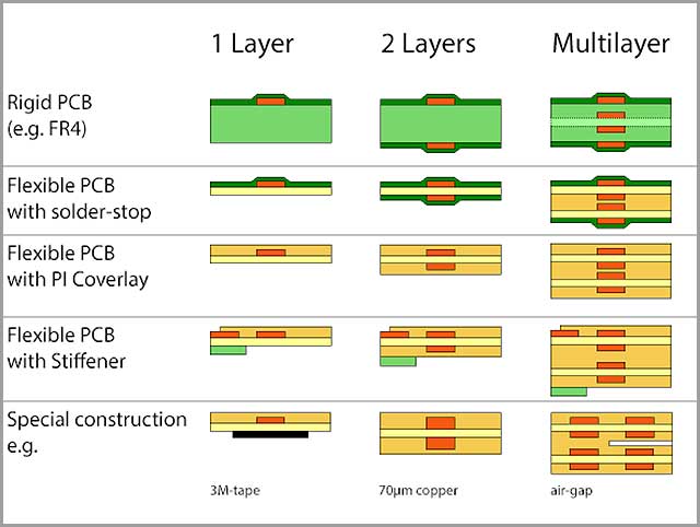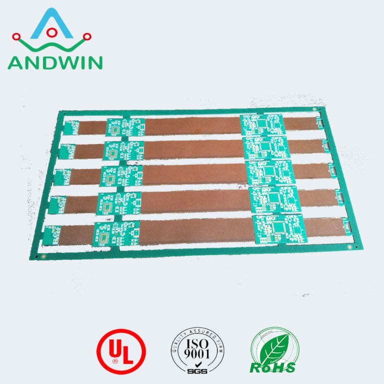
All flex pcb
Advantages Of Using Flex PCBs In Modern Electronics
In the rapidly evolving landscape of modern electronics, the demand for more compact, efficient, and versatile components has never been greater. Among the innovations meeting this demand, flexible printed circuit boards (flex PCBs) have emerged as a pivotal technology. These flexible circuits offer a myriad of advantages that make them indispensable in contemporary electronic design and manufacturing. As we delve into the benefits of flex PCBs, it becomes evident why they are increasingly favored over traditional rigid circuit boards.
To begin with, one of the most significant advantages of flex PCBs is their inherent flexibility.
Unlike rigid PCBs, which are confined to a fixed shape, flex PCBs can be bent, folded, and twisted to fit into unconventional spaces. This adaptability is particularly beneficial in the design of compact and portable devices, such as smartphones, wearable technology, and medical implants, where space is at a premium. The ability to conform to various shapes and contours allows designers to create more ergonomic and aesthetically pleasing products without compromising on functionality.
Moreover, flex PCBs contribute to a reduction in weight and volume, which is crucial in applications where size and weight are critical factors.
By eliminating the need for connectors and cables that are typically required in rigid board assemblies, flex PCBs streamline the design, resulting in lighter and more compact devices. This reduction in weight and volume not only enhances the portability of electronic devices but also improves their performance by minimizing the potential for mechanical failure due to fewer interconnections.
In addition to their physical advantages, flex PCBs offer superior reliability and durability.
The materials used in their construction, such as polyimide or polyester films, provide excellent resistance to environmental stressors, including heat, moisture, and vibration. This resilience ensures that flex PCBs maintain their integrity and functionality even in harsh conditions, making them ideal for use in automotive, aerospace, and industrial applications where reliability is paramount. Furthermore, the reduced number of solder joints in flex PCBs decreases the likelihood of connection failures, thereby enhancing the overall reliability of the electronic system.
Another noteworthy benefit of flex PCBs is their potential for cost savings in the long run.
While the initial design and manufacturing costs may be higher compared to rigid PCBs, the overall cost-effectiveness of flex PCBs becomes apparent when considering their longevity and reduced need for maintenance. The durability and reliability of flex PCBs translate into fewer repairs and replacements, ultimately leading to lower lifecycle costs. Additionally, the streamlined design process and reduced assembly time contribute to cost savings in production.
As we consider the advantages of flex PCBs, it is also important to acknowledge their role in fostering innovation.
The flexibility and versatility of these circuits open up new possibilities for electronic design, enabling the development of cutting-edge technologies that were previously unattainable with rigid boards. From foldable smartphones to advanced medical devices, flex PCBs are at the forefront of technological advancement, driving the evolution of modern electronics.
In conclusion, the advantages of using flex PCBs in modern electronics are manifold. Their flexibility, reduced weight and volume, enhanced reliability, cost-effectiveness, and potential for innovation make them an invaluable component in the design and manufacture of contemporary electronic devices. As technology continues to advance, the role of flex PCBs is likely to expand, further solidifying their position as a cornerstone of modern electronic design.
Design Considerations For Flex PCB Applications
In the realm of modern electronics, the demand for compact, lightweight, and versatile components has led to the increasing adoption of flexible printed circuit boards (PCBs). These all-flex PCBs offer a unique set of advantages, including the ability to bend and fold, which makes them ideal for a wide range of applications, from consumer electronics to medical devices. However, designing these flexible circuits requires careful consideration of several factors to ensure optimal performance and reliability.
To begin with, material selection is a critical aspect of flex PCB design.
Unlike rigid PCBs, which are typically made from fiberglass-reinforced epoxy, flex PCBs are constructed using flexible substrates such as polyimide or polyester. These materials provide the necessary flexibility while maintaining electrical integrity. Designers must choose the appropriate substrate based on the application’s environmental conditions, such as temperature and humidity, as well as mechanical stress factors. Polyimide, for instance, is favored for its excellent thermal stability and chemical resistance, making it suitable for high-performance applications.
In addition to material selection, the layout of the circuit traces plays a pivotal role in the design of flex PCBs.
The traces must be carefully routed to minimize stress and prevent cracking or delamination during bending. It is advisable to use curved traces instead of sharp angles, as this reduces stress concentration points. Furthermore, maintaining a consistent trace width and spacing is essential to ensure uniform current distribution and avoid potential hotspots. Designers often employ staggered or offset trace patterns to enhance flexibility and durability.
Another important consideration is the bend radius, which refers to the minimum radius that the flex PCB can be bent without causing damage.
The bend radius is influenced by factors such as the thickness of the substrate and the number of layers in the PCB. A smaller bend radius allows for tighter bends, which is advantageous in compact designs. However, exceeding the recommended bend radius can lead to mechanical failure. Therefore, it is crucial to adhere to manufacturer guidelines and conduct thorough testing to determine the optimal bend radius for a specific application.
Moreover, the choice of adhesive and coverlay materials is vital in protecting the flex PCB from environmental factors and mechanical wear.
The coverlay, typically made from polyimide or polyester, serves as a protective layer that shields the circuit from moisture, dust, and abrasion. The adhesive used to bond the coverlay to the substrate must be compatible with the materials and capable of withstanding the operating conditions. Selecting the right combination of adhesive and coverlay materials ensures the longevity and reliability of the flex PCB.
Thermal management is another key aspect that cannot be overlooked in flex PCB design.
As electronic devices become more powerful, they generate more heat, which can adversely affect the performance and lifespan of the components. Effective thermal management strategies, such as incorporating thermal vias or using heat-dissipating materials, are essential to dissipate heat efficiently and maintain optimal operating temperatures.
In conclusion, designing all-flex PCBs requires a comprehensive understanding of material properties, mechanical constraints, and environmental factors. By carefully considering these design elements, engineers can create flexible circuits that meet the demands of modern electronic applications while ensuring reliability and performance. As technology continues to evolve, the role of flex PCBs in enabling innovative and compact designs will undoubtedly expand, making them an indispensable component in the electronics industry.
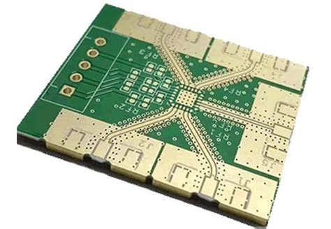
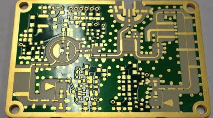
Manufacturing Process Of Flexible Printed Circuit Boards
The manufacturing process of flexible printed circuit boards (FPCBs) is a sophisticated and intricate procedure that requires precision and expertise. FPCBs are essential components in modern electronics, offering flexibility, lightweight properties, and the ability to fit into compact spaces. The process begins with the selection of appropriate materials, which is crucial for ensuring the performance and reliability of the final product. Typically, polyimide films are chosen for their excellent thermal stability and mechanical properties, serving as the substrate upon which the circuit is built.
Once the substrate is selected, the next step involves the application of a conductive layer, usually copper, onto the polyimide film.
This is achieved through a process known as lamination, where the copper foil is bonded to the substrate under heat and pressure. Following this, a photoresist layer is applied to the copper surface. The photoresist is a light-sensitive material that plays a critical role in defining the circuit pattern. By exposing the photoresist to ultraviolet light through a photomask, the desired circuit design is transferred onto the board. The areas exposed to light become hardened, while the unexposed regions remain soft and can be washed away, revealing the underlying copper.
Subsequently, the exposed copper is etched away using a chemical solution, leaving behind the circuit pattern protected by the hardened photoresist.
This etching process is a pivotal stage, as it determines the precision and accuracy of the circuit paths. After etching, the remaining photoresist is stripped away, exposing the clean copper traces that form the circuit. To protect these traces and enhance the board’s durability, a solder mask is applied. This layer not only insulates the copper traces but also prevents solder bridges during component assembly.
The next phase involves drilling holes for vias and through-hole components.
These holes are typically created using laser drilling or mechanical drilling, depending on the design requirements and the thickness of the board. Once the holes are drilled, they are plated with copper to establish electrical connections between different layers of the circuit. This step is crucial for multi-layer FPCBs, where inter-layer connectivity is essential for the board’s functionality.
Following the drilling and plating processes, the FPCB undergoes a series of inspections and tests to ensure quality and performance.
These inspections include visual checks, electrical testing, and sometimes even X-ray analysis to verify the integrity of the connections and the absence of defects. Any discrepancies found during these inspections are addressed before proceeding to the final stages of manufacturing.
The final steps in the manufacturing process involve cutting the FPCB to its desired shape and size, followed by the application of surface finishes.
These finishes, such as gold or silver plating, are applied to enhance solderability and protect the copper from oxidation. Once the surface finish is applied, the FPCB is ready for component assembly and integration into electronic devices.
In conclusion, the manufacturing process of flexible printed circuit boards is a meticulous and multi-step procedure that demands attention to detail and adherence to stringent quality standards. From material selection to final inspection, each stage plays a vital role in producing FPCBs that meet the high-performance requirements of modern electronic applications. As technology continues to advance, the demand for flexible and reliable circuit solutions will only grow, underscoring the importance of mastering this complex manufacturing process.
Common Challenges And Solutions In Flex PCB Design
In the realm of modern electronics, flexible printed circuit boards (flex PCBs) have emerged as a pivotal innovation, offering unparalleled versatility and adaptability. However, designing flex PCBs presents a unique set of challenges that require careful consideration and strategic solutions. Understanding these challenges and their corresponding solutions is crucial for engineers and designers aiming to optimize the performance and reliability of their flex PCB applications.
One of the primary challenges in flex PCB design is managing the mechanical stress that these circuits endure.
Unlike rigid PCBs, flex PCBs are subjected to bending, folding, and twisting, which can lead to mechanical fatigue and eventual failure. To address this, designers must carefully select materials that offer both flexibility and durability. Polyimide is a popular choice due to its excellent thermal stability and mechanical properties. Additionally, incorporating strain relief features, such as curved traces and filleted corners, can significantly reduce stress concentrations and enhance the longevity of the circuit.
Another significant challenge is ensuring signal integrity in flex PCBs.
The flexible nature of these circuits can introduce issues such as impedance mismatches and electromagnetic interference (EMI). To mitigate these problems, designers should employ controlled impedance techniques and utilize ground planes to provide a return path for signals, thereby minimizing EMI. Furthermore, maintaining consistent trace widths and spacing is essential to prevent signal degradation. Advanced simulation tools can be invaluable in predicting and addressing potential signal integrity issues before the physical prototype stage.
Thermal management is also a critical consideration in flex PCB design.
The compact and flexible nature of these circuits often leads to higher component densities, which can exacerbate heat dissipation challenges. Effective thermal management strategies include the use of thermal vias, heat sinks, and thermal interface materials to facilitate heat transfer away from critical components. Additionally, selecting materials with high thermal conductivity can help in managing heat more efficiently.
Moreover, the manufacturing process of flex PCBs introduces its own set of challenges.
The delicate nature of flexible substrates requires precise handling and processing to avoid damage. Ensuring proper alignment during the lamination process is crucial to prevent misregistration, which can lead to circuit failures. Collaborating closely with experienced manufacturers who understand the nuances of flex PCB production can help mitigate these risks and ensure high-quality outcomes.
Cost considerations also play a significant role in flex PCB design.
While the benefits of flexibility and space savings are clear, the materials and processes involved can be more expensive than those for traditional rigid PCBs. To address this, designers should focus on optimizing the layout to minimize material usage and reduce waste. Additionally, leveraging design for manufacturability (DFM) principles can streamline production processes and lower costs.
In conclusion, while flex PCB design presents a range of challenges, understanding these issues and implementing strategic solutions can lead to successful and reliable applications. By carefully managing mechanical stress, ensuring signal integrity, addressing thermal management, navigating manufacturing complexities, and considering cost implications, designers can harness the full potential of flex PCBs. As technology continues to advance, the demand for innovative and adaptable electronic solutions will only grow, making the mastery of flex PCB design an increasingly valuable skill in the electronics industry.