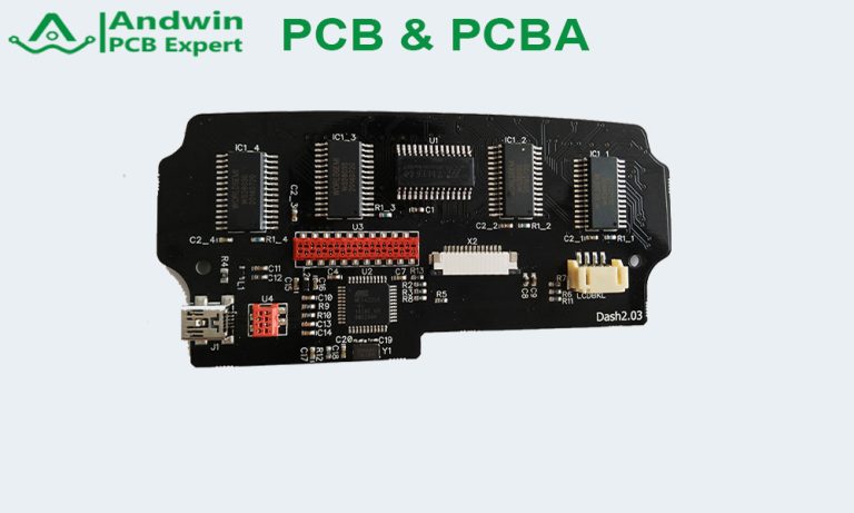
altium create flex pcb
Basic steps to create flexible PCB in Altium Designer
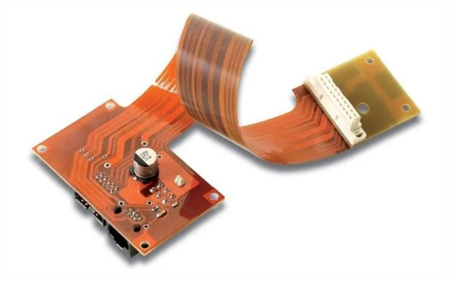
In modern electronic design, flexible printed circuit boards (Flex PCB) are becoming more and more popular due to their unique advantages. As a powerful electronic design automation software, Altium Designer provides designers with comprehensive tools to create flexible PCBs. This article will introduce the basic steps to create flexible PCBs in Altium Designer in detail to help designers better master this process.
First, start Altium Designer and create a new PCB project.
After the project is created, enter the PCB editor and start defining the basic parameters of the flexible PCB. By setting the layer stack structure of the PCB, you can specify the flexible and rigid areas. Typically, a flexible PCB consists of a multi-layer structure, which includes flexible layers and rigid layers. By adding and configuring these layers in the “Layer Stack Manager”, designers can accurately define the material and thickness of each layer.
Next, designers need to clearly define the boundaries of the flexible and rigid areas in the PCB design.
Using the “Region” tool, you can draw the outlines of different regions in the PCB layout. By setting the properties of these regions, designers can specify which parts are flexible and which parts are rigid. This step is critical to ensure the functionality and reliability of the flexible PCB.
After defining the flexible and rigid areas, designers can start to place components and routing.
Unlike traditional rigid PCBs, the routing of flexible PCBs needs to take into account bending and folding factors. Therefore, right-angle turns should be avoided as much as possible when routing, and smooth curves should be used to reduce stress concentration. In addition, designers should pay attention to maintaining signal integrity and electrical performance to ensure that the flexible PCB can operate normally under various working conditions.
To further optimize the design of flexible PCBs, designers can use the simulation tools provided by Altium Designer for verification. Through simulation, potential problems can be detected and adjustments can be made to improve the reliability and performance of the design. For example, using thermal simulation tools can evaluate the performance of flexible PCBs under different temperature conditions to ensure that they will not overheat or fail in actual applications.
Finally, after completing the design and performing simulation verification, designers can generate manufacturing files.
Altium Designer provides a variety of file formats to facilitate communication and collaboration with manufacturers. When generating manufacturing files, designers should pay special attention to the special requirements of flexible PCBs, such as bending radius and inter-layer alignment, to ensure a smooth manufacturing process.
In short, creating a flexible PCB in Altium Designer requires a series of delicate steps, from defining the stackup structure to arranging components and wiring, to simulation verification and generating manufacturing files.
By following these steps, designers can take full advantage of flexible PCBs and design high-performance, high-reliability electronic products.
How to design multi-layer flexible PCB in Altium In modern electronic design, flexible printed circuit board (Flex PCB) is increasingly favored by engineers due to its lightness, flexibility and high density.
As a powerful electronic design automation software, Altium Designer provides comprehensive tools and functions for designing multi-layer flexible PCB.
First of all, the first step to design multi-layer flexible PCB is to create a new PCB project. In Altium, users can start a new project by selecting the “New Project” option under the “File” menu. Next, the user needs to define the number of layers and material properties of the project, which can be configured in detail in the “Layer Stack Manager”.`
When defining the stacking structure, users need to pay special attention to the selection of flexible materials and the adhesive between layers.
Altium provides a rich material library, and users can choose the right material according to design requirements. In addition, users can also customize material properties to ensure that the designed flexible PCB can meet specific mechanical and electrical performance requirements.
Next, users need to select “Define Board Shape” under the “Design” menu to define the shape and size of the PCB. For flexible PCBs, the definition of shape is particularly important because it directly affects the bending and installation of the circuit board.
After completing the board shape definition, users can start placing components and routing.
Altium provides a powerful component library and routing tools, and users can easily place components in the right position and use the automatic routing function to optimize the circuit layout. During the routing process, users need to pay special attention to the bending area of the flexible PCB, and avoid placing sensitive components or critical signal lines in these areas to prevent breakage or signal interference during the bending process.
In addition, Altium also provides a 3D view function, and users can switch to the 3D view at any time during the design process to check the overall layout and bending effect of the circuit board. This function is particularly important for the design of flexible PCBs, because it can help users find potential problems in advance and make corresponding adjustments. Finally, after completing the design, users need to perform electrical rule checks (ERC) and design rule checks (DRC) to ensure that the design of the circuit board meets the specifications and there are no electrical and mechanical errors. Altium’s ERC and DRC tools can automatically detect problems in the design and provide detailed reports to help users quickly correct errors.
In short, designing multi-layer flexible PCBs in Altium is a systematic process that requires users to carefully consider factors such as material selection, stacking structure, component placement and wiring at each step. By making full use of the various tools and functions provided by Altium, users can efficiently complete the design of flexible PCBs and ensure their reliability and performance in practical applications.
Best Practices for Flexible PCB Design Using
In modern electronic design, flexible printed circuit boards (Flex PCBs) are becoming increasingly popular due to their unique advantages. When designing flexible PCBs using Altium Designer, following some best practices can significantly improve design efficiency and product quality.
First, it is critical to understand the basic characteristics of flexible PCBs. Flexible PCBs are lightweight, bendable, and durable, and are suitable for applications where space is limited or where frequent bending is required. Therefore, in the early stages of design, clarifying the design requirements and application environment is the key to success.
Next, choosing the right material and stacking structure is an important step in designing flexible PCBs. Altium provides a rich material library and stacking templates, and designers can choose the right material and stacking method according to specific needs. For example, for applications that require high flexibility, polyimide (PI) materials and single-layer or double-layer structures can be selected. In addition, a reasonable stacking design can effectively reduce signal interference and electromagnetic compatibility issues.
In the layout and routing stage, following some basic principles can help optimize the design. First, try to avoid routing in the bending area, because bending will stress the wire, which may cause breakage or performance degradation. Second, keep the width and spacing of the wires consistent to ensure signal integrity and reliability. Altium provides powerful routing tools and rule checking functions to help designers automatically detect and fix potential problems.
In addition, when designing flexible PCBs, reasonable mechanical design cannot be ignored. Using Altium’s 3D view function, you can intuitively view and adjust the shape and size of the PCB to ensure that it perfectly matches the housing and other components. At the same time, adding appropriate stiffeners and support structures can improve the mechanical strength and durability of the flexible PCB.
After completing the design, comprehensive simulation and verification are the last step to ensure the success of the design. Altium provides a variety of simulation tools that can comprehensively analyze electrical, thermal and mechanical properties. Through simulation, potential problems can be discovered and solved in advance to avoid failures in actual production.
In short, when using Altium for flexible PCB design, following the above best practices can significantly improve design efficiency and product quality. From material selection, stackup design, layout and wiring to mechanical design and simulation verification, every link needs to be carefully considered and optimized. By making rational use of Altium’s powerful functions, designers can easily cope with various challenges of flexible PCB design and ultimately achieve high-performance and high-reliability products. Common errors and solutions when designing flexible PCB in Altium When designing, designers often encounter some common mistakes that not only affect the quality of the design, but may also cause production problems. However, by understanding these common mistakes and their solutions, designers can complete the design of flexible PCBs more effectively.
First, many designers ignore the importance of material selection when designing flexible PCBs. The materials of flexible PCBs are very different from rigid PCBs, and improperly selected materials may cause the board to break or degrade when bent. Therefore, designers should carefully select materials suitable for flexible applications, such as polyimide or polyester, and ensure that these materials can meet the mechanical and electrical requirements of the design.
Next, another common mistake is to ignore the design of the bending area. In flexible PCBs, the bending area is the most prone to problems. If not designed properly, the bending area may cause the board to break or poor signal transmission. To avoid this problem, designers should use wider wires in the bending area and avoid placing too many components in these areas. In addition, using bending radius guidelines, such as the minimum bending radius should be ten times the board thickness, can effectively reduce bending stress.
In addition, many designers ignore thermal management issues when designing flexible PCBs. Flexible PCBs are often used in high-density and high-power applications. If the heat management is not done properly, it may cause the board to overheat, which will affect its performance and life. To solve this problem, designers should consider the heat dissipation path in the design and use thermal conductive materials or heat sinks to effectively manage the heat.
Another common mistake is failing to properly handle the stackup structure. The stackup structure of flexible PCBs is very different from that of rigid PCBs, and designers need to pay special attention to the design of the stackup structure to ensure the flexibility and reliability of the board. In Altium, designers can use stackup management tools to define and optimize the stackup structure to ensure that the thickness and material of each layer meet the design requirements.
Finally, many designers ignore manufacturing tolerances and assembly issues when designing flexible PCBs. The manufacturing and assembly process of flexible PCBs is very different from that of rigid PCBs, and designers need to consider manufacturing tolerances and assembly requirements to ensure that the board can be produced and assembled smoothly. To do this, designers should work closely with manufacturers to understand their manufacturing and assembly capabilities and consider these factors in their designs.
In summary, when designing flexible PCBs in Altium, designers need to pay attention to issues such as material selection, bending area design, thermal management, stacking structure, and manufacturing tolerances. By understanding these common errors and their solutions, designers can more effectively complete the design of flexible PCBs to ensure their performance and reliability.
Material Selection and Performance Optimization of Flexible PCBs in Altium Designer
When designing flexible PCBs, material selection and performance optimization are crucial links. Altium Designer provides a wealth of tools and resources to help engineers make informed decisions in this process. First, choosing the right substrate is key to ensuring the performance of flexible PCBs. Common flexible substrates include polyimide (PI) and polyester (PET), of which polyimide is widely used due to its excellent thermal stability and mechanical properties. In contrast, although polyester is lower in cost, it does not perform as well as polyimide in high temperature environments. Therefore, choosing the right substrate according to the specific application environment is the first step to optimize the performance of flexible PCBs.
Next, the conductive material
The choice of conductive material is equally important. Copper foil is the most commonly used conductive material with good conductivity and processability. However, in some high-frequency applications, silver paste or other conductive polymers may be more suitable because they can provide lower resistance and higher signal integrity. In addition, the thickness of the conductive material also needs to be carefully considered. Thicker copper foil can carry more current, but it will increase the rigidity of the flexible PCB and affect its bending performance. Therefore, a balance needs to be found between conductivity and flexibility during the design process.
In order to further optimize the performance of flexible PCBs, the design of the laminate structure cannot be ignored. Multi-layer flexible PCBs can increase the density and complexity of circuits by increasing the number of layers, but this will also increase the difficulty and cost of manufacturing. Altium Designer provides powerful multi-layer design capabilities, allowing engineers to easily manage and optimize laminate structures during the design process. In addition, reasonable interlayer connection design, such as the use of blind and buried vias, can effectively reduce signal transmission paths and improve circuit performance.
In addition to material selection and laminate structure design, the optimization of the mechanical properties of flexible PCBs is also an important aspect. The bending radius is a key indicator for measuring the mechanical properties of flexible PCBs. Too small a bending radius may cause the substrate and conductive materials to break, thus affecting the reliability of the circuit. Altium Designer provides a detailed bending radius calculation tool to help engineers ensure that the mechanical properties of flexible PCBs meet the requirements during the design process.
Finally, thermal management is also an important part of flexible PCB design. Since flexible PCBs are often used in high-density and high-power electronic devices, good thermal management can effectively extend the service life of the circuit. Selecting a substrate with high thermal conductivity and a reasonable heat dissipation design, such as adding heat dissipation holes and heat sinks, can significantly improve the thermal performance of flexible PCBs.
In summary, Altium Designer provides comprehensive support for material selection and performance optimization of flexible PCBs. From the selection of substrates and conductive materials, to the optimization of laminate structure and mechanical properties, to the design of thermal management, engineers can use these tools and resources to design flexible PCBs with excellent performance and high reliability. Through reasonable material selection and optimized design, flexible PCBs can play their unique advantages in various complex applications.