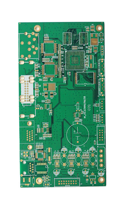
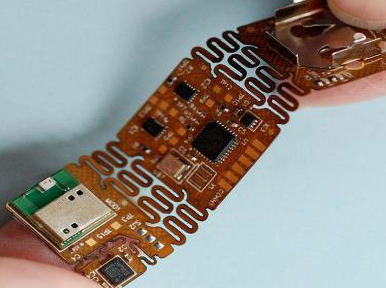
altium flex pcb example
Basic steps for Flex PCB design in Altium Designer
In modern electronic design, flexible printed circuit boards (Flex PCBs) are increasingly favored by designers due to their unique advantages, such as lightness, bendability, and high-density wiring. As a powerful electronic design automation (EDA) tool, Altium Designer provides comprehensive support for Flex PCB design. This article will introduce the basic steps for Flex PCB design in Altium Designer to help designers better master this technology.
First, creating a new PCB project is the starting point for designing Flex PCB. In Altium Designer, users can create a new project by selecting “New Project” from the “File” menu. Next, you need to add a new PCB document to the project, which can be achieved by right-clicking the project name and selecting the “PCB” option in “Add New to Project”.
Next, defining the flexible area is one of the key steps in Flex PCB design. In the PCB document, users can define the shape of the board by selecting “Define Board Shape” through the “Design” menu. Then, through the “Layer Stack Manager” option in the “Design” menu, users can define different layer stack structures for different areas. By adding and configuring flexible layers, designers can specify which areas are flexible and which are rigid.
After defining the flexible area, routing and component placement are the next important tasks. Altium Designer provides powerful routing tools that allow users to seamlessly transition between flexible and rigid areas. By using the “Interactive Routing” tool, designers can easily route between different layers and ensure signal integrity and electrical performance. In addition, the placement of components also requires special attention, especially in the flexible area, the layout of components should avoid excessive bending and mechanical stress.
In order to ensure the manufacturability of the design, it is essential to perform design rule checking (DRC). In Altium Designer, users can perform this operation by selecting “Design Rule Check” from the “Tools” menu. DRC will help identify potential problems such as minimum spacing violations, unconnected nets, etc., thereby ensuring that the design meets manufacturing requirements.
Finally, generating manufacturing files is the last step to complete the Flex PCB design. Through the “Fabrication Outputs” option in the “File” menu, users can generate necessary manufacturing files such as Gerber files, drill files, and assembly drawings. These files will be sent to PCB manufacturers for the production of actual circuit boards.
In summary, Flex PCB design in Altium Designer involves several key steps, from project creation, flexible area definition, routing and component placement, to design rule checking and generating manufacturing files. By following these steps, designers can take full advantage of Flex PCB and design high-performance and reliable electronic products. I hope that the introduction of this article can provide valuable guidance for your Flex PCB design. How to Optimize Signal Integrity for Flex PCBs in altium
Signal integrity is a critical factor when designing Flexible Printed Circuit Boards (Flex PCBs). Altium Designer provides a variety of tools and techniques to optimize signal integrity, ensuring that the board will work reliably in the actual application. First, it is crucial to understand the basic concepts of signal integrity. Signal integrity involves the signal maintaining its shape and quality during transmission, avoiding distortion and interference. To achieve this goal, designers need to pay attention to factors such as impedance matching, signal path length, and electromagnetic interference (EMI).
Next, impedance matching is one of the key steps to optimize signal integrity. In Altium, designers can use impedance control tools to ensure that the impedance of the signal path matches the impedance of the source and load. By setting the appropriate line width and layer spacing, the impedance can be effectively controlled. In addition, Altium also provides simulation tools to verify the impedance in the design phase to avoid problems in the manufacturing phase.
Then, the signal path length is also an important factor affecting signal integrity. When designing Flex PCB, the length of the signal path should be as short as possible to reduce signal delay and reflection. Altium’s automatic routing tools can help designers optimize signal paths to ensure the shortest transmission distance. At the same time, designers can also manually adjust the path of key signals to further optimize signal integrity.
In addition, electromagnetic interference (EMI) is another issue that needs attention. To reduce EMI, designers can use shielding and grounding layers in Altium. By adding shielding layers around key signal paths, the impact of external interference on the signal can be effectively reduced. The grounding layer can provide a stable reference voltage to further improve the stability of the signal. Altium also provides EMI simulation tools that can evaluate and optimize electromagnetic interference during the design phase.
Finally, designers should also pay attention to the mechanical properties of flexible circuit boards. Since Flex PCBs need to bend and fold in actual applications, the impact of these mechanical stresses on signal integrity needs to be considered during design. Altium provides 3D views and mechanical simulation tools to help designers evaluate and optimize the mechanical properties of circuit boards during the design phase, thereby ensuring that good signal integrity can be maintained in actual applications.
In summary, optimizing the signal integrity of Flex PCBs requires comprehensive consideration of multiple factors, including impedance matching, signal path length, electromagnetic interference, and mechanical characteristics. By making full use of the various tools and techniques provided by Altium Designer, designers can effectively optimize signal integrity during the design phase, thereby ensuring that the circuit board can work reliably in actual applications.
Best Practices for Flex PCB Design with Altium
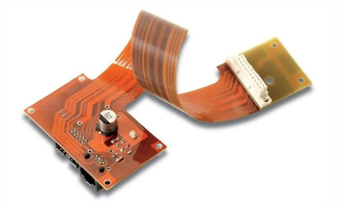
In modern electronic design, flexible printed circuit boards (Flex PCBs) are increasingly favored by designers due to their lightweight, flexible, and efficient features. When designing Flex PCBs with Altium Designer, following some best practices can significantly improve the quality and efficiency of your design. First, it is critical to understand the unique characteristics of Flex PCBs. Unlike traditional rigid PCBs, Flex PCBs can be bent and folded, which makes them very useful in space-constrained applications. However, this flexibility also brings design challenges, such as the need to consider bending radius and stress distribution.
Before starting the design, clarifying the design requirements and application environment is the first step. Through detailed discussions with customers or team members, determine the specific purpose, working environment, and mechanical requirements of the Flex PCB. This information will help you make more informed decisions during the design process. Next, choose the right material and stacking structure. Flex PCBs usually use polyimide (PI) or polyester (PET) as the substrate, which have good flexibility and heat resistance. According to the application requirements, choose the right material and number of layers to ensure that the circuit board can withstand the expected mechanical stress during use.
In Altium Designer, reasonable layout and routing are the key to successfully designing Flex PCBs. First, try to avoid placing components and vias in the bending area, because these areas will be subject to greater mechanical stress when bending, which may cause electrical connection failure. Second, use the bending radius tool to ensure that the bending radius in the design meets the manufacturer’s requirements. Generally, the bending radius should be at least ten times the thickness of the board to avoid excessive stress concentration.
In addition, optimizing the routing path to reduce stress concentration is also an important consideration. Try to use smooth curves instead of right-angle turns, which can reduce stress concentration points and extend the service life of the circuit board. For critical signal lines, consider using differential pair routing to improve signal integrity and anti-interference capabilities.
After completing the preliminary design, simulation and verification are key steps to ensure the reliability of the design. Using Altium Designer’s simulation tools, you can simulate the electrical performance and mechanical stress distribution of the circuit board under different bending states. Through these simulations, potential problems can be discovered in advance and adjusted before manufacturing.
Finally, work closely with manufacturers to ensure that the design meets manufacturing processes and quality standards. Clearly mark key parameters and requirements in the design files, such as bending radius, material type, and number of layers, so that manufacturers can accurately understand and implement the design intent. By following these best practices, Flex PCB design using Altium Designer will become more efficient and reliable, laying a solid foundation for the success of the final product.
Common Problems and Solutions for Flex PCB in Altium Designer
When using Altium Designer for Flex PCB design, designers often encounter some common problems. Understanding these problems and their solutions can not only improve design efficiency, but also ensure the quality and reliability of the final product. First of all, a problem that designers often face is material selection. The material of Flex PCB is different from that of traditional rigid PCB, and polyimide (PI) or polyester (PET) is usually used as the substrate. These materials have good flexibility and heat resistance, but their thickness, temperature resistance and electrical properties need to be considered when selecting. To solve this problem, designers should choose the right material according to the specific application requirements and conduct a detailed material evaluation at the beginning of the design.
Next, another common problem is the wiring and stacking design. Since Flex PCB needs to maintain the stability of electrical connections when bending and folding, the wiring design is particularly important. Designers should avoid arranging too many wires in the bending area and try to use rounded corner transitions to reduce stress concentration. In addition, the stacking design also needs special attention. It is usually recommended to use a single-layer or double-layer design in the bending area to reduce interlayer stress. Through reasonable wiring and stacking design, the reliability of Flex PCB can be effectively improved.
In addition, welding and assembly are also a key link in Flex PCB design. Due to the flexible characteristics of Flex PCB, warping and deformation problems are prone to occur during welding and assembly. To solve this problem, designers can add support structures to the welding area or use special fixtures for fixing. At the same time, choosing the right welding process and parameters can also effectively reduce deformation and damage during welding.
Finally, testing and verification are key steps to ensure the success of Flex PCB design. After the design is completed, comprehensive electrical performance testing and mechanical performance testing can be carried out to discover and solve potential problems. Especially in bending and folding tests, designers should simulate the actual use environment to ensure that the Flex PCB can work properly under various working conditions. Through rigorous testing and verification, the quality and reliability of the final product can be ensured.
In short, when designing Flex PCB in Altium Designer, designers need to comprehensively consider multiple aspects such as material selection, wiring and stacking design, welding and assembly, and testing and verification. Through reasonable design and optimization, common problems can be effectively solved and the design efficiency and product quality of Flex PCB can be improved. I hope these solutions can provide valuable references for designers and help them achieve better results in Flex PCB design.