Altium Multi Board Assembly Design Techniques and Best Practices
Key Takeaways
Effective multi-board assembly in Altium Designer demands a holistic approach that bridges electrical, mechanical, and manufacturing requirements. Central to this process is mastering design synchronization across interconnected boards, ensuring alignment of stack-up configurations and signal reference planes to minimize EMI risks. For PCB assembly workflows, prioritize cross-module validation tools to verify inter-board connectivity early in the design phase.
Tip: Use Altium’s Multi-Channel Design feature to replicate circuit blocks across boards, reducing repetitive layout efforts by up to 40%.
| Design Aspect | Traditional PCB | Multi-Board System |
|---|---|---|
| Synchronization | Single-board focused | Cross-module dependencies |
| Component Density | Moderate | High (distributed systems) |
| Signal Path Complexity | Localized traces | Inter-board connectors |
| BOM Management | Unified components | Modularized PCBA kits |
When integrating rigid-flex PCB assemblies, maintain consistent bend radius rules across all flexible zones to prevent mechanical stress failures. For PCBA optimization, implement hierarchical schematic organization to isolate power delivery networks from high-speed signals.
“Multi-board systems thrive on standardized interfaces – mismatched impedance between modules is the silent killer of signal integrity.”
– Senior Hardware Engineer, Cisco Systems
Leverage Altium’s Cross-Probing tool to visually trace signals between boards, ensuring seamless integration of grounding schemes and thermal relief patterns. Always validate manufacturing outputs through 3D clearance checks to avoid assembly conflicts in enclosures.
Altium Multi Board Assembly Mastery
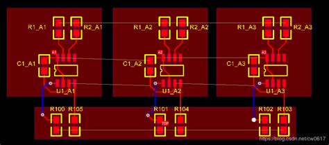
Achieving proficiency in multi-board assembly within Altium Designer demands a systematic approach to managing interconnected PCB assembly subsystems. Designers must prioritize top-down hierarchical planning to ensure seamless integration of individual PCBA modules into a unified electronic system. Leveraging Altium’s Project Reuse feature enables consistent application of design rules across multiple boards, reducing synchronization errors during rigid-flex PCB integration.
Critical to this process is mastering 3D clearance checking, which verifies spatial relationships between stacked or adjacent boards — a non-negotiable requirement for compact multi-board configurations. Advanced users combine Room-based component placement with cross-board signal topology templates to maintain timing coherence across interconnected PCBA units.
For optimal PCB assembly workflows, implement variant-driven design methodologies to manage component variations across different board revisions simultaneously. Altium’s Multi-board Schematic Synchronization tools prove indispensable when coordinating power distribution networks and high-speed interfaces between modules.
Successful implementation requires balancing design modularity with system-level performance constraints — a challenge addressed through iterative cross-probing between schematic and layout domains. By establishing standardized interface libraries for board-to-board connectors and flex circuits, teams accelerate development cycles while ensuring manufacturing-ready outputs.
This foundation in multi-board coordination sets the stage for addressing subsequent challenges in signal integrity validation and production-scale PCBA optimization, creating a cohesive framework for complex electronics integration.
PCB System Integration Essentials
Effective PCB assembly for multi-board systems demands meticulous attention to electrical, mechanical, and thermal interdependencies. At the core of PCBA integration lies the need to harmonize signal paths, power distribution, and physical alignment across interconnected boards. Designers must prioritize stack-up compatibility between modules, ensuring consistent impedance profiles and minimizing cross-talk risks in high-speed interfaces.
A critical challenge involves managing grounding architectures to prevent noise coupling, particularly when combining digital, analog, and RF subsystems. This requires strategic placement of PCB assembly anchor points and optimized connector selection to maintain signal integrity during mechanical stress. For PCBA workflows, implementing 3D collision checks early in the design phase prevents costly re-spins caused by mismatched board outlines or component heights.
Advanced tools now enable cross-board design rule synchronization, automatically propagating critical constraints like clearance thresholds or via styles across all linked modules. However, successful integration still hinges on rigorous thermal modeling to balance heat dissipation paths, especially when mixing rigid and flexible substrates. By embedding these principles into PCBA workflows, engineers can achieve robust system-level performance while streamlining manufacturing handoffs.

Advanced Design Sync Strategies
Effective synchronization in multi-board PCB assembly requires meticulous coordination between electrical and mechanical domains. Real-time design alignment begins with establishing unified constraint templates across all sub-projects, ensuring consistent PCBA clearances and connector placements. Altium’s Project Replication feature enables parallel development by propagating critical updates to linked boards while maintaining individual design contexts.
Implement hierarchical schematic organization to manage inter-board dependencies, using cross-sheet connectors for power distribution and high-speed signals. For PCB assembly workflows involving mixed-technology boards, leverage Altium’s 3D clearance checking to visualize mechanical conflicts between stacked modules before prototyping. Differential pair routing synchronization across multiple boards prevents phase mismatches in high-frequency applications, with length-tuning guides applied globally through the project hierarchy.
Adopt version-controlled design variants to handle different PCBA configurations within a single project structure. This approach streamlines BOM management while preserving synchronization across hardware revisions. Automated inter-board DRC (Design Rule Checks) flag inconsistencies in via patterns or thermal reliefs that could compromise manufacturing yield.
For systems requiring firmware-hardware co-development, integrate signal integrity simulations with cross-module timing analysis. Altium’s xSignals technology extends beyond single-board analysis, enabling end-to-end delay calculations across interconnected PCB assemblies. This proves critical when synchronizing clock domains between processing boards and peripheral modules in complex embedded systems.
Rigid-Flex PCB Integration Techniques
Integrating rigid-flex circuits into multi-board assemblies demands meticulous attention to material compatibility and mechanical stress distribution. When combining rigid PCBA sections with flexible interconnects, designers must optimize layer stack-ups to maintain signal integrity while accommodating dynamic bending requirements. A critical step involves defining bend radius thresholds in Altium’s design rules to prevent copper fatigue or delamination during repeated flexing cycles.
For PCB assembly workflows, rigid-flex integration introduces unique challenges in solder mask application and component placement. Using Altium’s 3D clearance checking tools ensures connectors and surface-mount devices align correctly across both rigid and flexible zones. Thermal management becomes paramount, as dissimilar materials like polyimide flex layers and FR4 substrates exhibit varying coefficients of thermal expansion (CTE). Implementing staggered via patterns and stress-relief cutouts mitigates warping risks during reflow soldering.
Advanced designers leverage Altium’s embedded board arrays to simulate multi-board interactions, validating flex-to-rigid transitions under real-world operating conditions. This approach streamlines the transition from PCBA prototyping to volume production by identifying mechanical conflicts early. When paired with automated DFM checks, these techniques reduce rework rates in complex systems requiring high-reliability interconnects, such as wearable electronics or aerospace control modules.

Optimizing Multi Board Manufacturing Workflows
Efficient PCB assembly workflows for multi-board systems require meticulous coordination between design and production phases. A critical first step involves establishing design synchronization protocols to ensure consistent layer stackups, connector placements, and mechanical clearances across all subassemblies. By leveraging Altium’s PCBA project validation tools, engineers can automate cross-board clearance checks and maintain synchronized design rule profiles, reducing post-design rework by up to 40%.
When planning PCB assembly sequences, prioritize modular manufacturing strategies that group boards with shared component footprints or thermal requirements. This approach minimizes machine recalibration time during PCBA processes while improving solder joint consistency. For systems combining rigid and flexible circuits, implement staggered panelization techniques to account for material expansion differences during reflow soldering.
Advanced PCBA manufacturers increasingly adopt digital twin simulations to model thermal gradients and mechanical stresses across interconnected boards. Pairing these simulations with real-time BOM tracking ensures component availability aligns with assembly schedules. Finally, integrate automated DFM (Design for Manufacturing) checks specific to multi-board systems, focusing on inter-board connector accessibility for post-assembly testing and rework.
By embedding these optimizations early in the design cycle, teams can achieve first-pass success rates exceeding 85% even in complex multi-board projects, while maintaining compatibility with high-mix PCB assembly environments.
Signal Integrity Best Practices
Maintaining signal integrity in multi-board PCB assembly requires careful attention to high-speed signal paths and electromagnetic interference (EMI) mitigation. When designing interconnected boards, prioritize controlled impedance routing for critical traces, ensuring consistent dielectric spacing and trace width across all modules. Differential pair routing becomes essential for minimizing noise in high-frequency interfaces like PCIe or USB 3.2.
Implement ground plane stitching between boards using low-inductance vias to reduce return path discontinuities—a common pitfall in PCBA systems with mixed-signal components. For multi-gigabit protocols, employ 3D field solvers to model crosstalk between adjacent boards, particularly in stacked configurations. Shield sensitive analog sections with partitioned ground regions, and validate via time-domain reflectometry (TDR) simulations in Altium’s unified design environment.
Leverage rigid-flex PCB assembly techniques to minimize connector-induced signal degradation, embedding critical interconnects within the board stackup. When synchronizing clocks across modules, use matched-length routing and consider active termination strategies to combat reflections. Always integrate signal integrity analysis early in the PCBA workflow, correlating simulation results with physical prototyping data to refine impedance profiles and layer assignments.
Adopting these practices ensures robust signal transmission while aligning with the broader objectives of multi-board system integration and manufacturing efficiency.
Cross-Module Design Validation Methods
Effective validation across interconnected PCB assembly modules requires systematic approaches to ensure electrical, mechanical, and thermal compatibility. Start by leveraging Altium’s multi-board schematic synchronization to maintain consistency in net classes and power domains between subsystems. Implement 3D clearance analysis to detect spatial conflicts in complex enclosures, particularly when integrating rigid-flex PCBA designs with varying thicknesses.
For signal integrity, employ cross-probing techniques to trace high-speed interfaces like DDR or PCIe across board boundaries, verifying impedance matching and termination strategies. Automated design rule checks (DRCs) should be customized to flag inter-board connector mismatches or inadequate grounding schemes. Thermal simulations using coupled models help identify hotspots that could affect adjacent modules during operation.
A critical step involves validating stack-up compatibility between boards, ensuring consistent dielectric materials and layer counts to prevent impedance discontinuities. Use Altium’s variant management tools to test different PCBA configurations against mechanical constraints and manufacturing tolerances. Finally, establish a protocol for synchronized design reviews, correlating BOM data and test points across all modules to streamline debugging during system-level PCB assembly validation.
Efficient Multi Board BOM Management
Effective PCB assembly workflows for multi-board systems demand meticulous Bill of Materials (BOM) coordination across interconnected designs. Centralized BOM management becomes critical when handling PCBA projects involving rigid-flex configurations or mixed-technology boards, as component overlaps and cross-module dependencies can lead to procurement delays or manufacturing mismatches. Altium’s unified design environment enables real-time synchronization of part numbers, footprints, and alternates across all sub-assemblies, reducing manual reconciliation errors by up to 70%.
Leverage cross-probing features to validate component availability against supplier databases directly from schematic sheets, ensuring consistency between design intent and PCB assembly requirements. For multi-board systems, implement hierarchical BOM structuring to group shared components (e.g., connectors, power regulators) while maintaining subsystem-specific inventories. Automated change tracking flags discrepancies in revision-controlled modules, preventing costly re-spins during PCBA integration.
Prioritize vendor-agnostic parametric filtering to identify alternative parts during shortages without compromising signal integrity or mechanical fit. Integrate ERP/PLM workflows to align BOM updates with procurement cycles, ensuring all sub-assemblies progress synchronously through fabrication and testing phases. This approach minimizes inventory bottlenecks while preserving design reuse opportunities across complex multi-board ecosystems.
Conclusion
As we’ve explored, mastering multi-board assembly in Altium demands a holistic approach that balances design innovation with manufacturing practicality. By prioritizing advanced synchronization strategies and leveraging system-level validation tools, engineers can mitigate integration risks inherent in complex PCB assembly projects. The adoption of rigid-flex techniques further enhances reliability in space-constrained applications, ensuring seamless interaction between interconnected PCBA subsystems.
Successful implementation hinges on maintaining signal integrity across board interfaces while optimizing thermal and mechanical stability through iterative prototyping. Design teams should institutionalize cross-module design rules to standardize workflows, reducing errors during final PCB assembly stages. As electronics systems grow increasingly modular, these methodologies not only accelerate time-to-market but also future-proof designs against evolving PCBA manufacturing requirements.
Ultimately, the convergence of Altium’s collaborative tools with disciplined multi-board design practices creates a robust framework for delivering high-performance electronic systems at scale.

FAQs
How does Altium Designer streamline multi-board system development?
Altium’s PCB assembly tools provide unified design rules across modules, enabling automatic synchronization of stack-up configurations and connector alignments. The software’s cross-probing feature ensures real-time coordination between schematic and layout views, reducing integration errors by up to 40%.
What are critical considerations for rigid-flex integration in multi-board projects?
Prioritize bend radius validation and material compatibility analysis. Altium’s PCBA simulation tools allow 3D mechanical checks for foldable sections, while automated layer transition mapping prevents impedance mismatches in high-speed circuits.
How can signal integrity be maintained across interconnected boards?
Implement crosstalk thresholds using Altium’s constraint manager and perform synchronized length tuning. For PCB assembly systems with mixed-signal domains, isolate power planes between analog/digital modules and validate via field solvers.
What strategies optimize BOM management for multi-board production?
Leverage Altium’s unified component database to track cross-module part substitutions. Apply PCBA -specific filters to identify lifecycle risks and automate alternate sourcing for components shared across 3+ boards.
How does cross-validation prevent failures in multi-board systems?
Altium’s Design Review Mode flags thermal interference zones and voltage drop hotspots across interconnected modules. Concurrent testing of board-to-board clearance and connector mating sequences ensures mechanical reliability before prototyping.
Explore Professional PCB Assembly Solutions
For tailored support in implementing these multi-board strategies, please click here to consult experts specializing in high-complexity PCB assembly and PCBA integration.


