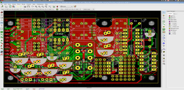
Altium usage – the meaning of each layer of PCB
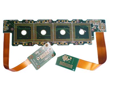
Altium’s PCB tool is used to convert schematics into PCBs.
a. Signal Layers: Signal layers include Top Layer, Bottom Layer, Mid Layer 1…30. These layers are all layers with electrical connections, that is, actual copper layers. The middle layer refers to the middle board layer used for wiring, and the wires are laid in this layer.
b. Internal Plane: Internal Plane 1…16, these layers are generally connected to the ground and power supply, becoming the power supply layer and ground layer, and also have electrical connection functions. They are also actual copper layers, but this layer is generally not wired and is composed of a whole piece of copper film.
c. Silkscreen Overlay: Including the top silkscreen layer (Top overlay) and the bottom silkscreen layer (Bottom overlay). The silkscreen characters that define the top and bottom layers are generally some text symbols printed on the solder mask layer, such as component names, component symbols, component pins and copyrights, etc., which are convenient for future circuit welding and error checking.
d. Paste Mask: Including the top paste layer and the bottom paste layer, it is a steel plate layer. This steel plate does not exist on the PCB, but is a tooling used for automated SMD welding, which is used to apply solder paste (Paste) to SMD.
If your board is not going to enter mass production, don’t consider this layer. It refers to the surface mount pads that we can see exposed outside, that is, the part that needs to be coated with solder paste before welding. Therefore, this layer is also useful when hot air leveling the pads and making welding steel mesh. (Solder is responsible for solder mask, and if you open a window to spray tin, you can do it in Solder. Paste is used to make steel mesh during reflow soldering. In fact, you don’t need to give this layer to the manufacturer when making boards)
e. Solder point layer (Solder Mask): Including the top solder mask layer (Top solder) and the bottom solder mask layer (Bottom solder). Its function is opposite to that of the solder paste layer. It refers to the layer that needs to be covered with green oil. All areas outside the defined area of this layer need to be covered with solder mask oil. This layer does not stick to solder, preventing the excess solder from short-circuiting adjacent soldering points during soldering. The solder mask covers the copper film wire to prevent the copper film from oxidizing too quickly in the air, but leaves space at the solder joints and does not cover the solder joints. (Solder, solder, welding)
f. Mechanical Layers: Up to 16 mechanical processing layers can be selected. To design a double-sided board, you only need to use the default option Mechanical Layer
1. (The mechanical layer is indeed used for edges and openings. If you draw openings in Keep-out and directly hand over the PcbDoc file to the manufacturer, the manufacturer will help to make this layer as a mechanical layer. But when you output Gerber yourself, it is best to define the openings in the mechanical layer.)
g. Keep Out Layer: Define the boundary of the wiring layer. After defining the keep-out layer, in the subsequent wiring process, wiring with electrical characteristics cannot exceed the boundary of the keep-out layer.
h. Drill Layer: includes Drill guide layer and Drill drawing layer, which are the drilling data. (What is the difference? If you don’t make Gerber by yourself, just ignore it and draw the component pads and vias)
f. Multi-layer: refers to all layers of the PCB board.
In a word: TopSolder, the top layer needs to be covered with tin (remove the green oil; Solder==welding).
TopPaste is just the opposite, the top layer needs to be covered with green oil. (You can’t solder on it).