Alumina PCB: A Comprehensive Guide to Ceramic-Based Printed Circuit Boards
Introduction
Printed Circuit Boards (PCBs) are the backbone of modern electronics, providing the necessary electrical connections and mechanical support for electronic components. While traditional PCBs are made from materials like FR-4 (a glass-reinforced epoxy laminate), advanced applications often require materials with superior thermal, electrical, and mechanical properties. Alumina PCBs, which use alumina (Al₂O₃) as the substrate material, have emerged as a preferred choice for high-performance applications. Alumina, a type of ceramic, offers excellent thermal conductivity, electrical insulation, and mechanical strength, making it ideal for use in demanding environments. This article provides a comprehensive overview of alumina PCBs, covering their properties, manufacturing process, applications, advantages, challenges, and future trends.
1. Understanding Alumina PCBs
Alumina PCBs are a type of ceramic PCB that use alumina as the base material. Alumina, also known as aluminum oxide, is a widely used ceramic material due to its excellent combination of properties. Alumina PCBs are particularly valued for their ability to handle high temperatures, dissipate heat efficiently, and provide reliable electrical insulation.
1.1 Key Properties of Alumina
- High Thermal Conductivity: Alumina has a thermal conductivity of around 24-28 W/m·K, which is significantly higher than that of traditional PCB materials like FR-4. This makes alumina PCBs ideal for applications requiring efficient heat dissipation.
- Excellent Electrical Insulation: Alumina is an excellent electrical insulator, with a dielectric strength of up to 20 kV/mm. This ensures reliable performance in high-voltage applications.
- Mechanical Strength: Alumina is a hard and durable material, with a flexural strength of around 300-400 MPa. This makes alumina PCBs resistant to mechanical stress and wear.
- Thermal Stability: Alumina can withstand high temperatures without degrading, making it suitable for use in harsh environments.
- Chemical Resistance: Alumina is resistant to most chemicals, ensuring long-term reliability in corrosive environments.
1.2 Structure of Alumina PCBs
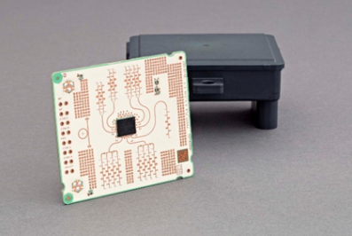
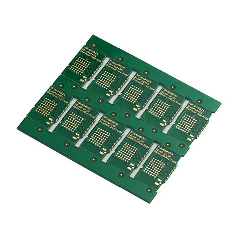
Alumina PCBs typically consist of a ceramic substrate (alumina) with one or more layers of conductive traces (usually copper) and insulating layers. The conductive traces are patterned to create the desired electrical connections, while the insulating layers provide electrical isolation between the traces.
2. Manufacturing Process of Alumina PCBs
The production of alumina PCBs involves several precise and controlled steps to ensure the quality and performance of the final product.
2.1 Substrate Preparation
The alumina substrate is prepared by mixing alumina powder with binders and sintering aids, followed by shaping and sintering at high temperatures (typically around 1600°C). The sintering process densifies the material, resulting in a strong and durable ceramic substrate.
2.2 Metallization
The alumina substrate is metallized to create the conductive traces. This can be done using various techniques, including thick-film printing, thin-film deposition, and direct bonded copper (DBC) technology.
- Thick-Film Printing: A conductive paste (usually containing silver or gold) is screen-printed onto the alumina substrate and then fired at high temperatures to form the conductive traces.
- Thin-Film Deposition: A thin layer of metal (such as copper or gold) is deposited onto the alumina substrate using techniques like sputtering or evaporation. The metal layer is then patterned using photolithography and etching.
- Direct Bonded Copper (DBC): A layer of copper is bonded directly onto the alumina substrate using a high-temperature oxidation process. The copper layer is then etched to create the desired circuit patterns.
2.3 Patterning and Etching
The conductive traces are patterned using photolithography, where a photoresist is applied to the metal layer, exposed to UV light through a mask, and then developed to create the desired pattern. The unwanted metal is then etched away using chemical etchants.
2.4 Via Formation
Vias are small holes drilled through the alumina substrate to create electrical connections between different layers of the PCB. The vias are typically filled with conductive material (such as copper) to ensure reliable electrical connections.
2.5 Quality Control
The final alumina PCB undergoes rigorous testing to ensure it meets the required specifications for thermal conductivity, electrical insulation, and mechanical strength. This includes visual inspection, electrical testing, and thermal cycling tests.
3. Applications of Alumina PCBs
Alumina PCBs are used in a wide range of industries and applications, thanks to their unique properties.
3.1 Power Electronics
Alumina PCBs are widely used in power electronic devices such as insulated gate bipolar transistors (IGBTs), power modules, and voltage regulators. Their high thermal conductivity and electrical insulation make them ideal for dissipating heat and ensuring reliable performance in high-power applications.
3.2 Automotive
In the automotive industry, alumina PCBs are used in electric vehicles (EVs) and hybrid electric vehicles (HEVs) for power inverters, motor drives, and battery management systems. Their ability to operate at high temperatures and withstand thermal cycling makes them suitable for the demanding conditions of automotive applications.
3.3 Aerospace and Defense
In aerospace and defense applications, alumina PCBs are used in radar systems, communication equipment, and power supplies. Their thermal stability and mechanical strength make them ideal for use in extreme conditions.
3.4 Industrial Electronics
Alumina PCBs are used in industrial electronics for motor drives, power supplies, and control systems. Their ability to dissipate heat and provide electrical insulation ensures reliable performance in industrial environments.
3.5 Medical Devices
Alumina PCBs are used in medical devices such as imaging systems, diagnostic equipment, and implantable devices. Their biocompatibility and chemical resistance make them suitable for use in medical applications.
3.6 Renewable Energy
Alumina PCBs are used in renewable energy systems such as solar inverters and wind turbines. Their high thermal conductivity and electrical insulation ensure efficient power conversion and reliable operation in harsh environments.
4. Advantages of Alumina PCBs
Alumina PCBs offer several advantages over traditional PCB materials, making them ideal for high-performance applications.
4.1 High Thermal Conductivity
The high thermal conductivity of alumina allows for efficient heat dissipation, reducing the risk of overheating and ensuring reliable performance in high-power applications.
4.2 Excellent Electrical Insulation
Alumina provides excellent electrical insulation, preventing short circuits and ensuring reliable performance in high-voltage applications.
4.3 Mechanical Strength
Alumina is a hard and durable material, making alumina PCBs resistant to mechanical stress and wear.
4.4 Thermal Stability
Alumina can withstand high temperatures without degrading, making it suitable for use in harsh environments.
4.5 Chemical Resistance
Alumina is resistant to most chemicals, ensuring long-term reliability in corrosive environments.
5. Challenges and Limitations
Despite their many advantages, alumina PCBs face several challenges and limitations.
5.1 Cost
The manufacturing process for alumina PCBs is complex and requires specialized equipment, which can increase the cost of the final product.
5.2 Brittleness
Alumina is inherently brittle and can be prone to cracking under mechanical stress. This limits its use in applications where impact resistance is critical.
5.3 Thermal Mismatch
Although the thermal expansion coefficient of alumina is closely matched to that of silicon, there can still be a mismatch with other materials used in electronic assemblies. This can lead to thermal stress and potential failure.
5.4 Manufacturing Complexity
The precise control required during the metallization and patterning processes makes the manufacturing of alumina PCBs complex and time-consuming.
6. Future Trends and Innovations
The field of alumina PCBs is continuously evolving, driven by advancements in materials science and manufacturing technologies.
6.1 Development of New Ceramic Materials
Researchers are exploring new ceramic materials with improved thermal and mechanical properties. For example, aluminum nitride (AlN) and silicon carbide (SiC) are being investigated as potential alternatives to alumina.
6.2 Advanced Metallization Techniques
New metallization techniques, such as laser-assisted metallization and additive manufacturing, are being developed to improve the quality and reliability of alumina PCBs.
6.3 Integration with Advanced Semiconductor Devices
The integration of alumina PCBs with advanced semiconductor devices, such as gallium nitride (GaN) and silicon carbide (SiC) power devices, is expected to drive innovation in power electronics.
6.4 Additive Manufacturing
Additive manufacturing (3D printing) is being explored as a method for creating complex alumina PCB components with integrated circuit patterns. This approach offers greater design flexibility and reduces material waste.
Conclusion
Alumina PCBs are a vital material in modern electronics, offering a unique combination of thermal conductivity, electrical insulation, and mechanical strength. Their applications span a wide range of industries, from power electronics and automotive systems to aerospace and medical devices. Despite the challenges associated with their cost, brittleness, and manufacturing complexity, ongoing research and development are driving innovations that promise to enhance the performance and expand the applications of alumina PCBs. As the demand for high-performance electronic systems continues to grow, alumina PCBs will play an increasingly important role in enabling the technologies of the future. By addressing the challenges and leveraging emerging technologies, manufacturers can unlock the full potential of alumina PCBs, driving progress in science and industry.

