An In-Depth Guide to OrCAD for PCB Design
Introduction
Printed Circuit Board (PCB) design is a critical aspect of electronic product development, and choosing the right design software can significantly impact efficiency, accuracy, and performance. OrCAD, developed by Cadence Design Systems, is one of the most widely used PCB design tools in the electronics industry. Known for its powerful schematic capture, simulation, and PCB layout capabilities, OrCAD provides engineers with a comprehensive solution for designing complex electronic circuits.
This article explores the key features of OrCAD, its advantages in PCB design, and best practices for utilizing the software effectively.
1. Overview of OrCAD
OrCAD is a suite of tools that includes:
- OrCAD Capture – Schematic design software for creating and editing circuit diagrams.
- OrCAD PSpice – A simulation tool for analyzing circuit behavior.
- OrCAD PCB Designer – A layout tool for designing and routing PCBs.
- OrCAD Sigrity – Signal and power integrity analysis for high-speed designs.
These tools work together to provide a seamless workflow from schematic entry to final PCB manufacturing.
2. Key Features of OrCAD
2.1 Schematic Capture with OrCAD Capture
OrCAD Capture is the foundation of the design process, allowing engineers to:
- Create hierarchical schematics for complex designs.
- Use an extensive library of components.
- Generate netlists for PCB layout and simulation.
- Perform Design Rule Checks (DRC) to identify errors early.
2.2 Circuit Simulation with OrCAD PSpice
PSpice is an industry-standard simulation tool that enables:
- Transient Analysis – Examining time-domain responses.
- AC/DC Analysis – Evaluating frequency and bias behavior.
- Monte Carlo Analysis – Assessing design robustness against component variations.
- Parametric Sweeps – Optimizing component values for performance.
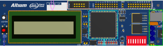
2.3 PCB Layout with OrCAD PCB Designer
The PCB layout module offers:
- Auto-interactive Routing – Smart routing for high-speed signals.
- Constraint Management – Defining design rules for trace width, spacing, and impedance.
- 3D Visualization – Viewing the PCB in three dimensions to check mechanical fit.
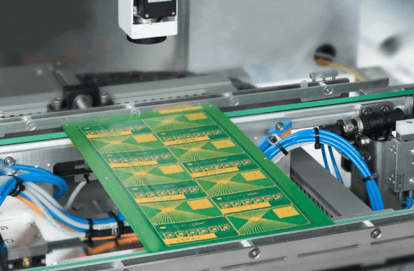
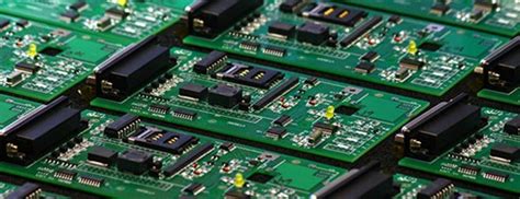
- Manufacturing Outputs – Generating Gerber files, drill files, and assembly drawings.
2.4 Signal and Power Integrity with OrCAD Sigrity
For high-frequency and high-speed designs, Sigrity provides:
- Impedance Analysis – Ensuring signal integrity.
- Power Delivery Network (PDN) Analysis – Optimizing power distribution.
- Crosstalk Analysis – Minimizing interference between traces.
3. Advantages of Using OrCAD for PCB Design
3.1 Industry-Standard Tool
OrCAD is widely adopted in the electronics industry, making it easier to collaborate with manufacturers and other engineers.
3.2 Seamless Integration
The integration between schematic capture, simulation, and PCB layout reduces errors and speeds up the design process.
3.3 High Accuracy and Reliability
Advanced simulation and DRC tools ensure that designs meet performance and manufacturing requirements.
3.4 Scalability
OrCAD supports designs ranging from simple single-layer boards to complex multi-layer high-speed PCBs.
3.5 Extensive Component Libraries
Pre-built libraries for common components save time and reduce manual entry errors.
4. Best Practices for PCB Design Using OrCAD
4.1 Organize Schematics Properly
- Use hierarchical blocks for complex circuits.
- Label nets clearly to avoid confusion during layout.
4.2 Leverage Simulation Early
- Run PSpice simulations before PCB layout to verify circuit behavior.
- Use Monte Carlo analysis to account for component tolerances.
4.3 Follow PCB Layout Guidelines
- Component Placement – Group related components to minimize trace lengths.
- Routing Strategies – Use differential pairs for high-speed signals.
- Ground Planes – Ensure a solid ground return path to reduce noise.
4.4 Perform Design Rule Checks (DRC)
- Check for unconnected nets, overlapping components, and manufacturing constraints.
4.5 Verify with 3D Models
- Use 3D visualization to check for mechanical conflicts with enclosures.
4.6 Generate Accurate Manufacturing Files
- Export Gerber files, drill files, and Bill of Materials (BOM) for fabrication.
5. Common Challenges and Solutions in OrCAD
5.1 Managing Large Schematics
- Solution: Use hierarchical design and modular blocks.
5.2 High-Speed Signal Integrity Issues
- Solution: Apply proper impedance matching and use Sigrity for analysis.
5.3 Component Footprint Errors
- Solution: Verify footprints in the library before placement.
5.4 Power Distribution Problems
- Solution: Optimize power planes and use decoupling capacitors.
6. Future Trends in PCB Design with OrCAD
As PCB technology evolves, OrCAD continues to integrate new features:
- AI-Driven Routing – Automated optimization of trace routing.
- Cloud Collaboration – Real-time teamwork on designs.
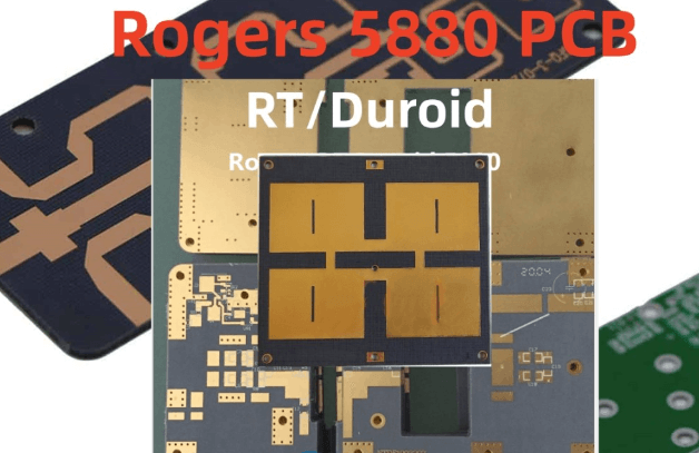
- Advanced Materials Support – Designing with flexible and high-frequency substrates.
Conclusion
OrCAD remains one of the most powerful and versatile PCB design tools available. Its seamless integration of schematic capture, simulation, and PCB layout makes it an essential tool for electronics engineers. By following best practices and leveraging OrCAD’s advanced features, designers can create high-performance, manufacturable PCBs efficiently.
As technology advances, OrCAD will continue to evolve, incorporating AI, cloud computing, and enhanced simulation capabilities to meet the demands of next-generation electronics.