Analysis of Causes of PCB Trace Breakage
Abstract
Printed Circuit Board (PCB) trace breakage is a common issue in electronic manufacturing and operation, leading to circuit failures and reduced product reliability. This paper explores the root causes of PCB trace breakage, including design flaws, manufacturing defects, environmental factors, and mechanical stresses. By understanding these causes, engineers can implement preventive measures to enhance PCB durability and performance.
1. Introduction
PCBs serve as the backbone of modern electronic devices, providing electrical connections between components. Trace breakage, where conductive pathways are interrupted, can result in device malfunction or complete failure. Identifying the root causes of trace breakage is crucial for improving PCB design, manufacturing processes, and operational longevity.
This paper categorizes the causes of PCB trace breakage into four main areas:
- Design-related causes
- Manufacturing defects
- Environmental and chemical factors
- Mechanical and thermal stresses
Each category is analyzed in detail to provide a comprehensive understanding of trace breakage mechanisms.
2. Design-Related Causes
2.1 Insufficient Trace Width
One of the primary causes of trace breakage is inadequate trace width. If a trace is too narrow, it may not withstand the current load, leading to overheating and eventual breakage. High-current traces require wider widths to prevent excessive resistance and thermal damage.
2.2 Poor Routing Practices
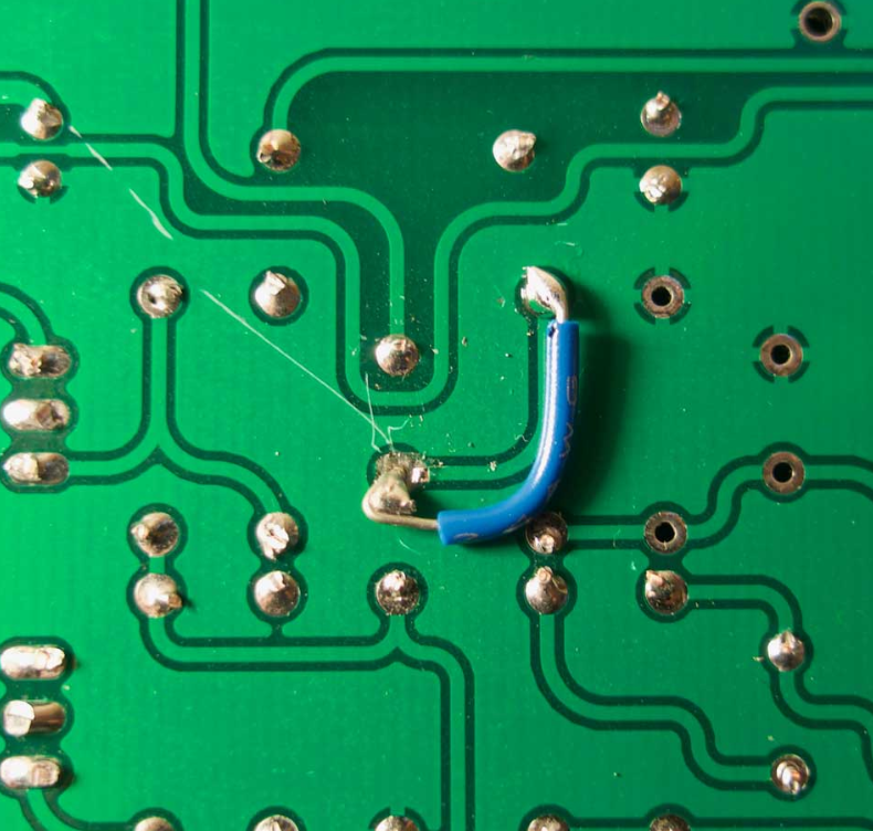
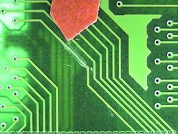
- Sharp Corners and Acute Angles: Traces with sharp turns can create high-stress points, increasing the risk of cracking.
- Inadequate Spacing: Traces placed too close to each other may suffer from electromigration or short circuits, weakening the structure over time.
- Via Placement: Excessive or improperly placed vias can weaken the PCB substrate, leading to trace fractures.
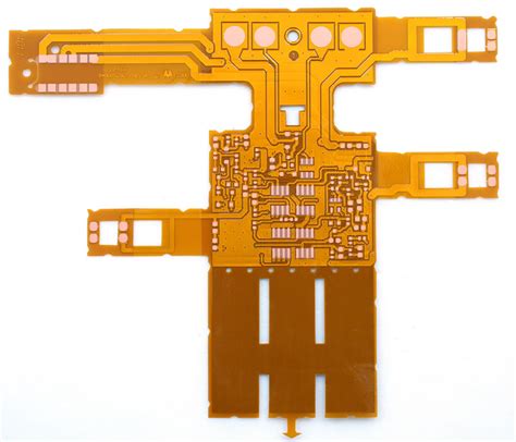
2.3 Lack of Strain Relief
Flexible PCBs or those subjected to vibration require strain relief features such as curved traces or additional support to prevent breakage.
3. Manufacturing Defects
3.1 Etching Issues
Over-etching or under-etching during PCB fabrication can lead to weak or incomplete traces:
- Over-etching: Reduces trace thickness, making them more susceptible to breakage.
- Under-etching: Leaves residual copper, potentially causing short circuits or uneven trace widths.
3.2 Copper Thickness Variations
Inconsistent copper plating during manufacturing can result in thin spots in traces, increasing the likelihood of breakage under mechanical or thermal stress.
3.3 Poor Lamination
Improper lamination of PCB layers can lead to delamination, where traces separate from the substrate, causing open circuits.
3.4 Solder Mask Issues
- Misalignment: Exposes traces to environmental damage.
- Brittleness: Cracks in the solder mask can propagate into the underlying traces.
4. Environmental and Chemical Factors
4.1 Moisture and Corrosion
- Humidity Absorption: PCBs exposed to high humidity can absorb moisture, leading to oxidation and corrosion of copper traces.
- Electrochemical Migration: Ionic contaminants (e.g., flux residues) can cause dendritic growth, leading to short circuits and trace degradation.
4.2 Chemical Exposure
- Acidic or Alkaline Environments: Harsh chemicals can corrode copper traces.
- Flux Residues: Improper cleaning after soldering can leave corrosive residues.
4.3 Thermal Cycling and Oxidation
Repeated heating and cooling cycles can cause expansion and contraction, weakening traces over time. Oxidation of exposed copper further accelerates trace degradation.
5. Mechanical and Thermal Stresses
5.1 Flexing and Bending
- Dynamic Flexing: Repeated bending (e.g., in flexible PCBs) can fatigue traces, leading to cracks.
- Improper Handling: Mechanical stress during assembly or installation can damage traces.
5.2 Vibration and Shock
PCBs in automotive or industrial applications are prone to vibration-induced fractures if not properly secured.
5.3 Thermal Stress
- Uneven Heating: Localized hotspots can weaken traces.
- Thermal Expansion Mismatch: Different materials in the PCB expand at different rates, causing stress on traces.
6. Preventive Measures
To mitigate PCB trace breakage, engineers should:
- Optimize trace width based on current requirements.
- Avoid sharp angles in trace routing.
- Ensure proper etching and copper thickness during manufacturing.
- Use conformal coatings to protect against moisture and chemicals.
- Implement strain relief in flexible PCBs.
- Conduct thorough testing (e.g., thermal cycling, vibration tests).
7. Conclusion
PCB trace breakage arises from multiple factors, including design flaws, manufacturing defects, environmental exposure, and mechanical stresses. By addressing these issues through improved design practices, stringent manufacturing controls, and protective measures, the reliability and lifespan of PCBs can be significantly enhanced. Future research should focus on advanced materials and AI-assisted design optimization to further reduce trace breakage risks.