Analysis of crosstalk problems in high-speed digital systems
With the continuous development of electronic technology, the frequency of signals in high-speed circuits has become higher, the edges have become steeper, the size of circuit boards has become smaller, and the density of wiring has become larger. These factors have made the signal integrity problem more and more prominent in the design of high-speed digital circuits, and it has become an inevitable problem for high-speed circuit design engineers.
Crosstalk refers to the transfer of harmful signals from one network to another. It is an important problem in signal integrity issues. It is common in digital design and may appear on devices such as chips, PCB boards, connectors, chip packages, and connector cables. If the crosstalk exceeds a certain limit, it will cause false triggering of the circuit, causing the system to fail to work properly. Therefore, it is very important for engineers to understand the mechanism of crosstalk problems and master the design methods to solve crosstalk.
1 Mechanism of crosstalk problems
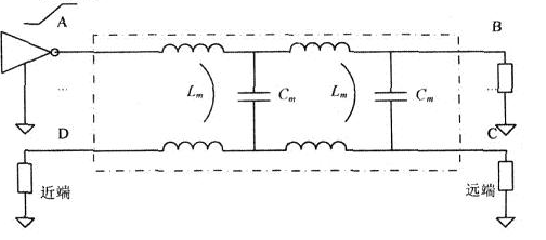
Crosstalk is the unwanted voltage or current noise interference generated on adjacent transmission lines due to electromagnetic coupling when the signal propagates on the transmission line. The edge field effect of the signal line is the root cause of the crosstalk. In order to facilitate analysis, several related concepts are introduced below. As shown in Figure 1, assuming that the driver at point A is the interference source and the receiver at point D is the interfered object, the transmission line where the driver A is located is called the interference source network or the offending network (Agreessor), and the corresponding transmission line network where the receiver D is located is called the static network or the victim network. The crosstalk at the end of the static network close to the interference source is called near-end crosstalk (also called backward crosstalk), and the crosstalk at the end far from the interference source is called far-end crosstalk (or forward crosstalk). Due to different causes, crosstalk can be divided into two categories: capacitive coupling crosstalk and inductive coupling crosstalk.
1.1 Capacitive coupling mechanism
When there is a signal transmission on the interference line, due to the change of the signal edge voltage, the distributed capacitance on the interference line will induce a time-varying electric field in the area near the signal edge, and the victim line is in this electric field, so the changing electric field will generate an induced current on the victim line.
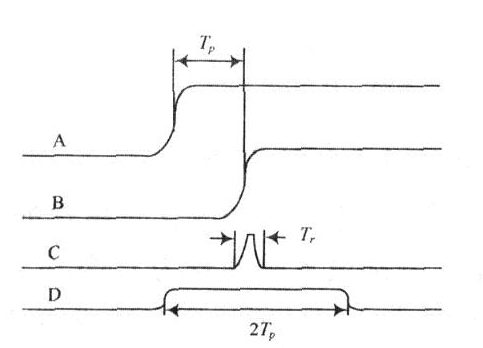
The edge of the signal can be regarded as a current source moving along the interference line. During its movement, current noise is continuously generated on the victim line through capacitive coupling. Since the impedance in each direction on the victim line is the same, 50% of the capacitive coupling current flows to the near end and the other 509/6 flows to the far end. In addition, the capacitive coupling current flows from the signal path to the return path, so the coupling current propagating to the near end and the far end is positive.
For near-end capacitive coupling crosstalk, as the rising edge pulse appears in the driver output signal, the current flowing to the near end will increase rapidly from zero. After the edge inputs a saturation length, the near-end current will reach a fixed value. In addition, the coupling current flowing to the near end will flow to the near end at a constant speed. When the rising edge reaches the receiving end of the interference line, this rising edge will be accepted and absorbed, and no coupling current signal will be generated. However, there is still a backward current on the victim line flowing to the near end of the victim line, so the coupling current at the near end will continue for twice the transmission delay.
For far-end capacitive coupling crosstalk, since the edge of the signal can be regarded as a moving current source, it will generate a coupling current flowing into the victim line through mutual capacitance in the area near the edge, and 50% of the generated coupling current will flow into the far end in the same direction and speed as the signal on the interference line.
Therefore, as the signal on the interference line is transmitted, the forward coupling current will be continuously generated on the victim line and will be continuously superimposed with the existing forward coupling current and transmitted to the far end together. Since crosstalk is only generated in the area near the edge of the signal, the duration of the coupling current flowing to the far end is equal to the transition time of the signal. The specific capacitive coupling is shown in Figure 2.
1.2 Inductive coupling mechanism
When the signal propagates on the interference line, due to the change of the signal current, a time-varying magnetic field will be generated in the area near the signal transition through the action of the distributed inductance. The changing magnetic field will induce a noise voltage on the victim line, thereby forming an inductive coupling current and propagating to the near end and the far end respectively. Unlike the capacitive coupling current, the direction of the inductive coupling current is opposite to the direction of signal propagation on the interference line. When transmitting to the near end, the current loop is from the signal path to the return path, while when transmitting to the far end, the current loop is from the return path to the signal path.
For near-end inductive coupling crosstalk, its characteristics are very similar to those of near-end capacitive coupling crosstalk.
It also increases rapidly from zero. When the transmission length is greater than or equal to the saturation length, it will stabilize at a fixed value and last for twice the transmission delay. Because the inductive coupling current flowing to the near end is in the same direction as the capacitive coupling current, the two will be superimposed together.
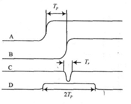
For far-end inductive coupling crosstalk, the inductive coupling noise has the same propagation speed as the signal edge on the interference line, and more and more noise current will be coupled out at each step, and the duration is equal to the signal jump time. However, since the current flow direction is opposite to the far-end capacitive coupling current, the coupling current reaching the far-end receiver of the victim line is the difference between the two. The specific inductive coupling is shown in Figure 3.
l.3 Mixed effect of mutual inductance and mutual capacitance
Generally, on a complete ground plane, the crosstalk voltages generated by capacitive and inductive coupling are equal in magnitude, so the total noise of far-end crosstalk cancels each other out due to the different polarities of capacitive and inductive coupling. In stripline circuits, a better balance between the two can be shown, and its far-end coupling coefficient is extremely small. However, for microstrip lines, since most of the electric field related to crosstalk passes through air rather than other insulating materials, capacitive crosstalk is smaller than inductive crosstalk, resulting in a small negative number for its far-end crosstalk coefficient.
2 Simulation analysis of crosstalk
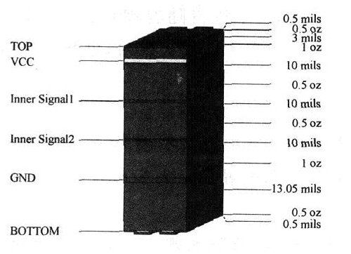
In actual design, board layer characteristics (such as thickness, dielectric constant, etc.) as well as line length, line width, line spacing, signal rise time, etc. will all affect crosstalk. The following uses Mentor Graphie’s signal integrity simulation software Hyperlynx to analyze the above factors affecting crosstalk. First, a two-line crosstalk model is established in Hyperlynx, as shown in Figure 4. The line width of the two lines is 5 mil, the line length is 6 in, and the line spacing is 5 mil. Both lines are top-layer microstrip lines with a characteristic impedance of 49.5Ω. Both lines are terminated with a 50Ω resistor to eliminate the influence of reflection. The driver of the interference line uses the IBIS model of CMOS process devices, with a voltage of 3.3 V and a frequency of 100 MHz. The dielectric constant of the PCB is 4.3, and it is a six-layer board. Its stacking structure is shown in Figure 5.
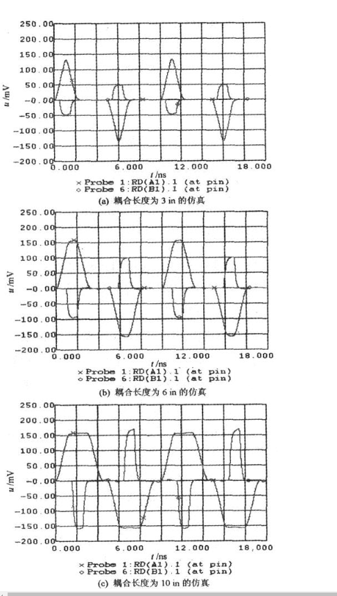
2.1 Effect of coupling length on crosstalk
Change the coupling length of the two lines, set the coupling length to 3 in, 6 in, and 10 in respectively, and keep other settings unchanged.
Figure 6 (a) is the crosstalk waveform with a coupling length of 3 in, where the near-end crosstalk peak is 126.34 mV and the far-end is 43.01 mV; Figure 6 (b) is the crosstalk waveform with a coupling length of 6 in, where the near-end crosstalk peak is 153.23 mV and the far-end is 99.46 mV; Figure 6 (c) is the crosstalk waveform with a coupling length of 10 in, where the near-end crosstalk peak is 153.23 mV and the far-end is 163.98 mV. It can be seen that the far-end crosstalk peak is proportional to the coupling length, and the longer the coupling length, the greater the crosstalk; while for the near-end crosstalk, when the coupling length is less than the saturation length, the crosstalk will increase with the increase of the coupling length, but when the coupling length is greater than the saturation length, the near-end crosstalk value will be a stable value.
2.2 The influence of line spacing on crosstalk
The following is to keep other settings unchanged and examine the influence of changes in line spacing on crosstalk. The line spacing is set to 5 mil and 15 mil respectively, and the simulation waveform is shown in Figure 7.
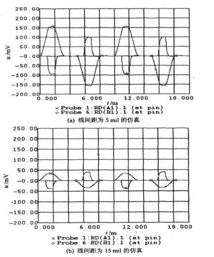
As shown in Figure 7, when the line spacing is 5 mil, the near-end crosstalk peak is 153.23 mV and the far-end is 99.46 mV; when the line spacing is 15 mil, the near-end crosstalk peak is 33.40 mV and the far-end is 40.49 mV. It can be seen that as the line spacing increases, both the near-end and far-end crosstalk will decrease. When the line spacing is greater than or equal to 3 times the line width, the crosstalk is already very small.
2.3 Effect of rise time on crosstalk
The following examines the effect of the change in rise time on crosstalk, and other settings remain unchanged. Set the driver to CMOS 3.3 V MEDI-UM; CMOS 3.3 V FAST; CMOS 3.3 V ULTRA-FAST respectively, and the simulation waveform is shown in Figure 8.
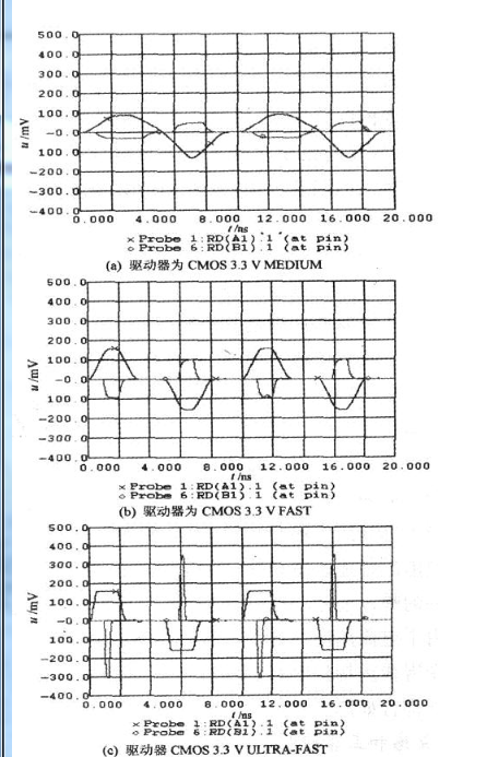
The near-end crosstalk peak in Figure 8(a) is 153.9 mV, and the far-end crosstalk is 46.3 mV; the near-end crosstalk peak in Figure 8(b) is 153.2 mV, and the far-end crosstalk is 99.5 mV; the near-end crosstalk peak in Figure 8(c) is 153.2 mV, and the far-end crosstalk is 349.9 mV. It can be seen that when the rise time is shortened, the far-end crosstalk noise becomes larger and larger. For near-end crosstalk, if the rise time is shorter than the delay of the transmission line, the near-end crosstalk is not related to the rise time; if the rise time is longer than the delay of the transmission line, the near-end crosstalk noise is related to the rise time (as the rise time decreases, the near-end crosstalk becomes larger).
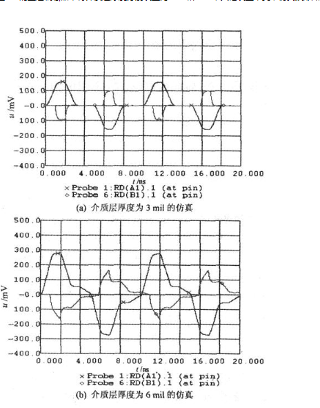
2.4 Effect of dielectric layer thickness on crosstalk
In the PCB stackup editor, the dielectric layer thickness is set to 3 mil and 6 mil respectively, and other settings remain unchanged. The simulation waveform is shown in Figure 9.
From the above simulation waveforms, we can see that when the thickness of the dielectric layer is 3 mil, the near-end crosstalk peak is 153.2 mV and the far-end crosstalk is 99.5 mV; when the thickness of the dielectric layer is 6 mil, the near-end crosstalk peak is 277.3 mV and the far-end crosstalk is 163.9 mV. It can be seen that as the thickness of the dielectric layer decreases, the crosstalk will also decrease.
3 Methods to solve crosstalk
Crosstalk is common in the design of electronic products. Through the above analysis and simulation, we understand the characteristics of crosstalk and summarize the following methods to reduce crosstalk:
(1) When conditions permit, try to increase the distance between traces, reduce the length of parallel traces, and use jog routing when necessary.
(2) While ensuring signal timing, try to select devices with slower rising and falling edges to slow down the speed of changes in the electric and magnetic fields, thereby reducing crosstalk.
(3) When designing traces, the conductor should be kept as close to the ground plane or power plane as possible. This allows the signal path to be tightly coupled with the ground plane, reducing interference to adjacent signal lines.
(4) When the wiring space allows, inserting a ground wire between two signal lines with severe crosstalk can reduce the coupling between the two signal lines, thereby reducing crosstalk.
4 Conclusion
Crosstalk is an important part of signal integrity, affecting the timing of the system, reducing the noise margin, and causing the system to not work properly. The mechanism of crosstalk in high-speed circuits is introduced, and the crosstalk is analyzed through simulation. The relationship between the size of the crosstalk and the factors affecting the crosstalk is obtained. On this basis, some methods to reduce crosstalk are proposed, which have certain guiding significance for solving the crosstalk problem in high-speed and high-density circuit design.


