Andwin PCB Customization
From precise laminate material selection to complex microvia drilling technology,Andwin’s PCB customization service provide robust technical support for high-end electronic Products.
In today’s rapidly evolving electronics industry,printed circuit boards(PCBS)serve as the core foundation of electronic devices ,and their design and manufacturing quality directly impact the performance and reliability of the entire product.Andwin PCB customization specializes in providing customers with highly specialized,flexible,and diverse PCB manufacturing solutions,meeting a wide range of needs,from simple prototypes to the most advanced electronic products.
Whether it’s aerospace equipment,medical instrument,or high-end communications systems,Andwin’s extensive technical capabilities and rigorous quality control ensure that every circuit board meets the most demanding application requirements.
1 What is Andwin PCB?Application and Core values
PCB customization refers to the process of designing and and manufacturing printed circuit board based on a customer’s specific needs.Unlike standard PCBs,custom PCBs take into account unique electrical characterisitcs,mechanical shapes,environmental compatibility,and specialized application requirements.
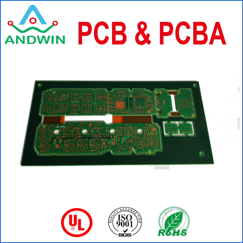
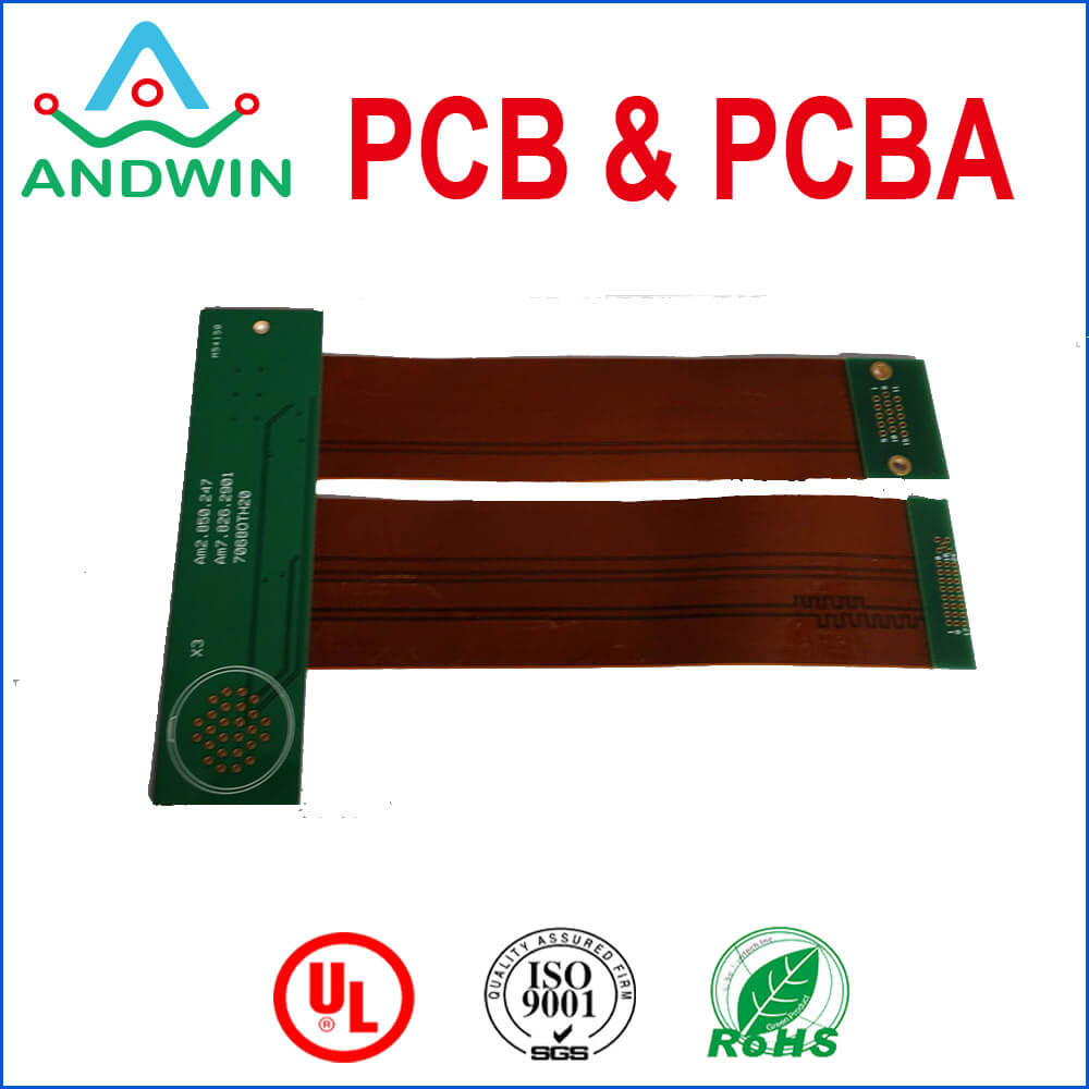
Andwin’s custom PCB services offer comprehensive manufacturing capabilities,supporting demanding board designs,including laser-drilled microvias,cavity boards,heavy copper(up to 20 ounces),solder-in-pad technology,microwave and RF boards,and multilayer designs with up to 40 layers.
These custom PCBs are widely used in a variety of high-end applications,including aerospace,defense,medical devices,communications infrastructure,and industrial automation.In these application,circuit reliability,performance,and durability are paramount and standard PCBs often fall short of these specialized requirements.
2.Key Technical Capabilities of Custom PCBs Laminate Material
Selection: Andwin offers a wide range of laminate material to meet diverse design and application requirements.These materials include:
RF material:For high-frequency applications such ad communication equipment.
RoHS-Compliant laminates:Meet environmental requirements.
Halogen-free materials:Suitable for environmentally sensitive applications.
Advanced signal integrity materials:For high-Frequency applications such as communications equipment.
Advanced HDI laminate:Support high-density interconnect designs.
Surface Finish Options:Electroplating consists of a precise amount of metal placed on uncovered exterior copper and plated through-holes.Andwin offter a variety of surface finish options:
- Leaded and lead-free hot air leveling(HASL)
- Electroless nickel and hard gold plating
- Electroless nickel electroless palladium gold(ENEPIG)
- Immersion silver and immersion tin
- Electroless nickel immersion
Electroless nickel
Advanced Manufacturing Processes: For more advanced custom PCB designs, ADWIN offers a variety of specialized processes:
Controlled dielectric: Precisely control dielectric constant and thickness.
Controlled impedance: Ensure signal integrity.
Plating baths and plated edges: Enhance connectivity and durability.
Countersunk and countersunk holes: For specialized mounting requirements.
Castellated holes: Facilitate board-to-board connections.
Depth-controlled drilling: Precisely control drilling depth.
3 .PCB Design Process: From Concept to Production
Design Preparation and Planning: PCB design is a systematic process that begins with defining the product’s electrical functionality and mechanical constraints. Electronic design automation (EDA) tools like Altium Designer (AD) provide comprehensive PCB design solutions, from schematic drawing and PCB layout to final manufacturing file output.
Before beginning design, you need to determine the number of PCB layers, dimensions, materials, and key components. This stage is particularly important for custom PCBs, as it determines the feasibility and cost of subsequent manufacturing.
Schematic Design: The schematic is the blueprint for the PCB design, using symbols to represent electronic components and lines to illustrate the electrical connections between them. In Altium Designer, you can use existing component libraries or create custom components.
For complex designs, a hierarchical schematic can be used to divide the entire system into multiple functional modules, making the design more modular and manageable.
PCB Layout and Routing: Once the schematic is complete and passes electrical rule checking (ERC), the next step is to convert it into a physical PCB layout. This process includes:
Defining the Board Outline: Draw the board outline on a mechanical layer or a keep-out layer.
Component Placement: Optimize component positions to reduce trace lengths and improve signal integrity.
Routing: Connect all components while adhering to design rules (such as line width and spacing).
Design Verification and Output: After routing is complete, design rule checking (DRC) and signal integrity analysis are performed to ensure the design meets all requirements. Manufacturing files (such as Gerber files, drill files, and mounting files) are then generated and sent to the PCB manufacturer for production.
4 Advantages and Industry Certifications of ADWIN Custom PCBs
Advantages of Custom PCBs: Choosing ADWIN’s custom PCB services offers several significant advantages:
Optimized Performance: Custom PCBs can be optimized for specific applications through precise control of impedance, signal integrity, and thermal management.
Improved Reliability: The use of high-quality materials and specialized processes enhances the PCB’s durability in harsh environments.
Space Efficiency: High-density interconnect (HDI) technology and multi-layer design enable more complex functionality within limited space.
Cost-Effectiveness: While the upfront investment is higher, an application-optimized design can reduce the cost of later modifications and failures.
Industry Certifications and Quality Standards: ADWIN holds numerous industry certifications and qualifications to meet demanding custom PCB requirements. These include:
IPC-A-600 Class 2/3: Requirements for high-performance and extended-life dedicated service electronic equipment.
MIL-PRF-31032: Certified for military applications.
MIL-PRF-55110: Standard for military/aerospace applications.
AS9100D: Aerospace Quality Management System.
ISO 9001: International Quality Management System Certification.
ITAR Registration: International Traffic in Arms Regulations Registered.
These certifications ensure that ADWIN’s custom PCB services meet the highest standards for military/aerospace, medical, and commercial applications.
5. How to Select Custom PCB Services: Considerations and Best Practices
Technical Capabilities Assessment: When selecting a custom PCB service provider, consider the following technical factors:
Laminate Material Selection: Does the supplier offer material options suitable for your application?
Advanced Process Support: Does the supplier support specialized processes such as HDI, microvias, and thick copper?
Manufacturing Precision: What are the process capabilities for minimum line width/line spacing, minimum aperture, etc.?
Quality Control: What testing equipment and quality assurance processes does the supplier have?
Business Considerations: In addition to technical capabilities, the following business factors should be considered:
Prototype and Mass Production Capabilities: Does the supplier have the capability to support prototypes all the way through mass production?
Delivery Time: Can your project timeline be met?
Cost Structure: Is the pricing transparent, and are there any hidden costs?
Customer Support: Is design support and technical consulting provided?
Design Preparation Tips: To ensure a smooth PCB customization project, please follow these best practices:
Provide complete design documentation: This includes Gerber files, drill diagrams, bill of materials (BOM), and assembly drawings.
Clarify Special Requirements: Communicate requirements for impedance control, surface finish, special testing, etc. in advance.
Conduct a Design for Manufacturability (DFM) review with the manufacturer before committing to manufacturing.
Consider Design for Manufacturability (DFM): Follow DFM principles to avoid designs that are difficult or costly to manufacture.
With the rapid development of the Internet of Things, 5G communications, and artificial intelligence technologies, the demand for high-performance, high-reliability PCBs will continue to grow. Emerging technologies such as flexible electronics, 3D-printed electronics, and embedded components are driving the PCB customization industry to new heights.
ADWIN PCB Customization Services will continue to be committed to technological innovation and quality improvement, helping customers meet increasingly complex electronic design challenges and transform their innovative ideas into real products.
In the future, we can expect to see more integrated functionality, higher density, and more environmentally friendly PCB solutions, driving the entire electronics industry towards a more advanced and sustainable direction.


