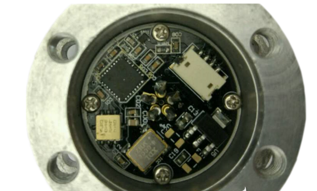
Any layer hdi pcb
Advantages Of Using HDI PCBs In Modern Electronics
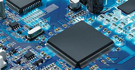
High-Density Interconnect (HDI) printed circuit boards (PCBs) have become a cornerstone in the advancement of modern electronics, offering a multitude of advantages that cater to the ever-evolving demands of technology. As electronic devices continue to shrink in size while increasing in functionality, the need for more efficient and compact circuit board designs has become paramount. HDI PCBs, with their ability to accommodate more components in a smaller area, provide an ideal solution to this challenge.
One of the primary advantages of using HDI PCBs is their ability to support higher component density.
By utilizing finer lines and spaces, smaller vias, and capture pads, HDI technology allows for more components to be placed on both sides of the board. This increased density is crucial for modern devices such as smartphones, tablets, and wearable technology, where space is at a premium. Consequently, manufacturers can design smaller, lighter, and more portable devices without sacrificing performance or functionality.
In addition to supporting higher component density, HDI PCBs also enhance electrical performance.
The shorter distances between components reduce signal loss and improve signal integrity, which is essential for high-speed applications. This is particularly beneficial in industries such as telecommunications and computing, where rapid data transmission and processing are critical. Furthermore, the use of microvias in HDI PCBs minimizes parasitic inductance and capacitance, leading to better overall electrical performance.
Another significant advantage of HDI PCBs is their contribution to improved thermal management.
As electronic devices become more powerful, they generate more heat, which can adversely affect performance and reliability. HDI PCBs, with their efficient use of space and materials, facilitate better heat dissipation. This is achieved through the use of thinner dielectric materials and strategically placed vias that help distribute heat more evenly across the board. As a result, devices can operate at optimal temperatures, enhancing their longevity and reliability.
Moreover, HDI PCBs offer greater design flexibility, which is a critical factor in the development of innovative electronic products.
The ability to incorporate multiple layers and blind or buried vias allows designers to create complex circuits that would be impossible with traditional PCB technology. This flexibility enables the integration of advanced features and functionalities, paving the way for cutting-edge applications in various fields, including medical devices, automotive systems, and aerospace technology.
In addition to these technical benefits, HDI PCBs also contribute to cost efficiency in the long run.
Although the initial manufacturing costs may be higher due to the complexity of the design and fabrication processes, the overall cost savings are significant. The reduction in size and weight of the final product leads to lower material and shipping costs. Furthermore, the enhanced performance and reliability of HDI PCBs result in fewer failures and less need for repairs or replacements, ultimately reducing maintenance costs.
In conclusion, the advantages of using HDI PCBs in modern electronics are manifold, ranging from higher component density and improved electrical performance to better thermal management and design flexibility. As technology continues to advance, the demand for more compact, efficient, and reliable electronic devices will only increase, solidifying the role of HDI PCBs as a vital component in the future of electronics.

Design Considerations For HDI PCB Manufacturing
When embarking on the design of High-Density Interconnect (HDI) printed circuit boards (PCBs), several critical considerations must be taken into account to ensure successful manufacturing and optimal performance. HDI PCBs, known for their compact design and high performance, are increasingly utilized in advanced electronics, including smartphones, tablets, and other compact devices. The design process for these intricate boards requires a meticulous approach, beginning with an understanding of the unique characteristics that distinguish HDI PCBs from traditional PCBs.
One of the primary considerations in HDI PCB design is the layer configuration.
HDI PCBs often incorporate multiple layers, which allow for a higher density of components and interconnections. This multi-layer approach facilitates the integration of more complex circuits within a smaller footprint. Designers must carefully plan the stack-up of these layers to optimize signal integrity and thermal management. The choice of materials for each layer is crucial, as it impacts the board’s overall performance and reliability. High-quality dielectric materials are often selected to ensure minimal signal loss and effective heat dissipation.
Transitioning from material selection to the layout design, the placement of vias is another critical aspect.
HDI PCBs utilize microvias, blind vias, and buried vias to connect different layers. These vias are significantly smaller than those used in traditional PCBs, allowing for more efficient use of space. However, their reduced size also necessitates precise drilling techniques and careful consideration of their placement to avoid signal interference and ensure robust connections. The strategic placement of these vias can significantly enhance the board’s electrical performance and reliability.
Moreover, the routing of traces in HDI PCBs demands careful attention.
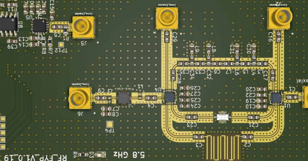
Due to the high density of components, trace routing becomes a complex task that requires advanced design software and expertise. Designers must ensure that traces are routed in a manner that minimizes electromagnetic interference and crosstalk, which can degrade signal quality. Additionally, the use of differential pairs and controlled impedance traces is often necessary to maintain signal integrity, especially in high-speed applications.
As we delve deeper into the design considerations, it is essential to address the aspect of thermal management.
HDI PCBs, with their compact design, can be prone to overheating if not properly managed. Effective thermal management strategies, such as the use of thermal vias and heat sinks, are crucial to dissipate heat efficiently and maintain the board’s performance. Designers must also consider the thermal expansion properties of the materials used, as mismatches can lead to mechanical stress and potential failure.
Furthermore, manufacturability is a key consideration in HDI PCB design.
The complexity of these boards requires advanced manufacturing techniques, such as laser drilling and sequential lamination. Designers must collaborate closely with manufacturers to ensure that the design is feasible and cost-effective to produce. This collaboration often involves iterative design reviews and adjustments to align with manufacturing capabilities and constraints.
In conclusion, the design of HDI PCBs is a multifaceted process that demands careful consideration of various factors, from layer configuration and via placement to trace routing and thermal management. By addressing these considerations with precision and expertise, designers can create HDI PCBs that meet the demanding requirements of modern electronic devices, ensuring high performance, reliability, and manufacturability. As technology continues to advance, the role of HDI PCBs in enabling compact and powerful electronic solutions will undoubtedly grow, underscoring the importance of thoughtful design practices in this field.

Comparing HDI PCBs To Traditional PCBs: Key Differences
High-Density Interconnect (HDI) printed circuit boards (PCBs) have become increasingly prevalent in the electronics industry, offering distinct advantages over traditional PCBs. As technology advances, the demand for more compact, efficient, and high-performing electronic devices has driven the evolution of PCB design. HDI PCBs, characterized by their higher wiring density per unit area, have emerged as a solution to meet these demands. To understand the key differences between HDI PCBs and traditional PCBs, it is essential to explore their structural, functional, and application-based distinctions.
One of the most notable differences between HDI and traditional PCBs lies in their structural design.
HDI PCBs utilize microvias, blind vias, and buried vias, which are significantly smaller than the through-hole vias used in traditional PCBs. This allows for a more compact design, enabling the placement of more components on a single board. Consequently, HDI PCBs can support more complex circuitry without increasing the board’s size. In contrast, traditional PCBs, with their larger vias, often require more layers to accommodate the same level of complexity, leading to increased board thickness and weight.
Furthermore, the materials used in HDI PCBs differ from those in traditional PCBs.
HDI boards often employ advanced materials with superior thermal and electrical properties, which enhance their performance in high-frequency applications. These materials contribute to better signal integrity and reduced electromagnetic interference, making HDI PCBs ideal for high-speed and high-frequency applications. Traditional PCBs, while still effective for many applications, may not offer the same level of performance in these demanding environments due to their reliance on conventional materials.
In addition to structural differences, the manufacturing processes for HDI and traditional PCBs also vary.
HDI PCBs require more advanced fabrication techniques, such as laser drilling for microvias and sequential lamination processes. These techniques allow for the precise placement of vias and traces, which is crucial for maintaining the integrity of high-density designs. On the other hand, traditional PCBs typically use mechanical drilling and simpler lamination processes, which are less costly but may not achieve the same level of precision required for complex designs.
The functional advantages of HDI PCBs over traditional PCBs are evident in their applications.
HDI technology is particularly beneficial in industries where space and weight are critical factors, such as in aerospace, medical devices, and consumer electronics. The ability to integrate more functionality into a smaller footprint allows for the development of compact, lightweight devices without compromising performance. Traditional PCBs, while still widely used in many applications, may not provide the same level of miniaturization and performance required in these cutting-edge fields.
Moreover, the cost implications of HDI versus traditional PCBs are an important consideration.
While HDI PCBs may have higher initial manufacturing costs due to their complex fabrication processes and advanced materials, they can offer cost savings in the long run. The reduced size and weight of HDI PCBs can lead to lower shipping and handling costs, as well as potential savings in assembly and integration processes. Traditional PCBs, with their simpler design and manufacturing processes, may be more cost-effective for less demanding applications where size and performance are not as critical.
In conclusion, the key differences between HDI and traditional PCBs are rooted in their structural design, materials, manufacturing processes, and applications. As the demand for more compact and efficient electronic devices continues to grow, HDI PCBs offer a viable solution by providing enhanced performance and miniaturization capabilities. While traditional PCBs remain relevant for many applications, the advantages of HDI technology make it an increasingly attractive option for industries seeking to push the boundaries of electronic design.
The Role Of HDI PCBs In Miniaturization Of Electronic Devices
High-Density Interconnect (HDI) printed circuit boards (PCBs) have become a cornerstone in the evolution of modern electronic devices, playing a pivotal role in the ongoing trend of miniaturization. As consumer demand for smaller, more powerful, and efficient devices continues to rise, the electronics industry has been compelled to innovate and adapt. HDI PCBs, with their advanced design and manufacturing techniques, have emerged as a critical solution to meet these demands.
To understand the significance of HDI PCBs in miniaturization, it is essential to first consider their unique characteristics.
Unlike traditional PCBs, HDI PCBs are designed with a higher density of interconnections, which allows for more components to be placed on a smaller board. This is achieved through the use of microvias, finer lines and spaces, and a greater number of layers. These features enable the integration of more complex circuitry within a limited space, which is crucial for the development of compact electronic devices.
Moreover, the use of HDI technology facilitates the reduction of signal loss and electromagnetic interference, which are common challenges in densely packed circuits.
By minimizing these issues, HDI PCBs enhance the performance and reliability of electronic devices. This is particularly important in applications where precision and efficiency are paramount, such as in medical devices, aerospace technology, and high-performance computing.
In addition to improving performance, HDI PCBs contribute to the miniaturization of electronic devices by enabling the integration of multiple functions into a single board.
This integration reduces the need for additional components and connectors, which not only saves space but also decreases the overall weight of the device. Consequently, manufacturers can produce lighter and more portable products without compromising on functionality or performance.
Furthermore, the versatility of HDI PCBs allows for their application across a wide range of industries.
In consumer electronics, for instance, smartphones, tablets, and wearable devices have all benefited from the compact and efficient design of HDI PCBs. These devices require a high level of functionality within a limited form factor, making HDI technology an ideal solution. Similarly, in the automotive industry, the demand for advanced driver-assistance systems (ADAS) and infotainment systems has driven the adoption of HDI PCBs, which support the integration of complex electronic systems within the confined spaces of modern vehicles.
As the trend towards miniaturization continues, the role of HDI PCBs is expected to expand further.
Advances in materials and manufacturing processes are likely to enhance the capabilities of HDI technology, enabling even greater levels of integration and performance. For instance, the development of flexible HDI PCBs could open new possibilities for innovative device designs, such as foldable smartphones and wearable technology that conforms to the human body.
In conclusion, HDI PCBs are indispensable in the miniaturization of electronic devices, offering a combination of high performance, reliability, and space efficiency. As technology continues to evolve, the importance of HDI PCBs in enabling the next generation of compact and powerful electronic devices cannot be overstated. Their ability to support complex circuitry within a small footprint makes them a vital component in the ongoing quest for innovation and advancement in the electronics industry.


