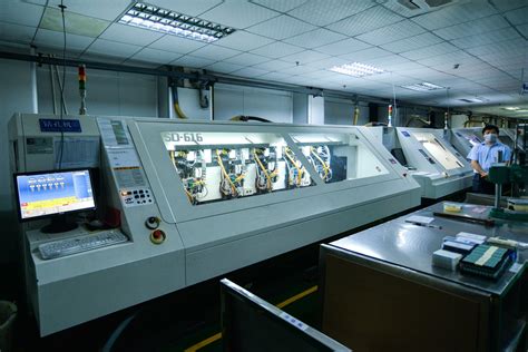
Aoi pcb assembly
Advantages Of AOI In PCB Assembly
Automated Optical Inspection (AOI) has become an indispensable tool in the realm of Printed Circuit Board (PCB) assembly, offering a multitude of advantages that significantly enhance the manufacturing process. As the demand for high-quality electronic devices continues to surge, the need for precise and efficient inspection methods has never been more critical. AOI addresses this need by providing a non-contact, automated solution that ensures the integrity and functionality of PCBs, thereby elevating the overall quality of electronic products.
One of the primary advantages of AOI in PCB assembly is its ability to detect defects early in the production process.
By identifying issues such as soldering defects, component misalignments, and missing components at an early stage, AOI helps prevent defective boards from progressing further down the production line. This early detection is crucial as it allows for immediate corrective actions, thereby reducing the likelihood of costly rework or scrapping of defective boards. Consequently, manufacturers can achieve higher yields and lower production costs, which is particularly beneficial in high-volume manufacturing environments.
In addition to early defect detection, AOI offers unparalleled accuracy and consistency in inspection.
Unlike manual inspection, which is prone to human error and fatigue, AOI systems utilize advanced imaging technology and sophisticated algorithms to perform precise and repeatable inspections. This high level of accuracy ensures that even the smallest defects are detected, which might otherwise go unnoticed during manual inspection. Moreover, the consistency provided by AOI systems ensures that every board is inspected to the same rigorous standards, thereby maintaining uniformity in product quality.
Another significant advantage of AOI is its speed and efficiency.
Traditional inspection methods can be time-consuming and labor-intensive, often requiring skilled operators to meticulously examine each board. In contrast, AOI systems can inspect multiple boards simultaneously and at a much faster rate, significantly reducing inspection times. This increased efficiency not only accelerates the overall production process but also allows manufacturers to meet tight deadlines and respond quickly to market demands. Furthermore, the automation of the inspection process frees up human resources, enabling them to focus on more complex and value-added tasks.
AOI also plays a crucial role in enhancing traceability and process control in PCB assembly.
Modern AOI systems are equipped with data collection and analysis capabilities, allowing manufacturers to gather valuable insights into the production process. By analyzing inspection data, manufacturers can identify trends and patterns that may indicate underlying issues in the production line. This information can be used to implement process improvements, optimize production parameters, and ultimately enhance the overall efficiency and quality of the manufacturing process. Additionally, the traceability provided by AOI systems ensures that any defects can be traced back to their source, facilitating root cause analysis and preventing recurrence.
Moreover, the integration of AOI into the PCB assembly process aligns with the broader trend towards Industry 4.0 and smart manufacturing.
AOI systems can be seamlessly integrated with other automated equipment and manufacturing execution systems (MES), creating a connected and intelligent production environment. This integration enables real-time monitoring and control of the production process, further enhancing efficiency and quality. As the electronics industry continues to evolve, the adoption of AOI and other advanced technologies will be essential in maintaining a competitive edge.
In conclusion, the advantages of AOI in PCB assembly are manifold, encompassing early defect detection, accuracy, efficiency, traceability, and process control. By leveraging the capabilities of AOI, manufacturers can ensure the production of high-quality PCBs, reduce costs, and enhance overall productivity. As technology continues to advance, the role of AOI in PCB assembly will undoubtedly become even more pivotal, driving further innovations and improvements in the manufacturing process.
How AOI Enhances Quality Control In PCB Manufacturing
Automated Optical Inspection (AOI) has become an indispensable tool in the realm of Printed Circuit Board (PCB) manufacturing, significantly enhancing quality control processes. As the demand for more complex and miniaturized electronic devices grows, the need for precise and reliable PCB assembly becomes paramount. AOI systems play a crucial role in ensuring that PCBs meet stringent quality standards, thereby reducing the risk of defects and improving overall product reliability.
To begin with, AOI systems utilize advanced imaging technologies to inspect PCBs at various stages of the manufacturing process.
These systems are equipped with high-resolution cameras and sophisticated algorithms that can detect a wide range of defects, including solder joint issues, component misalignments, and surface anomalies. By capturing detailed images of the PCB, AOI systems can compare the actual assembly against the intended design specifications, identifying any discrepancies with remarkable accuracy.
One of the primary advantages of AOI in PCB manufacturing is its ability to perform inspections at multiple stages, from pre-reflow to post-reflow and even during final assembly.
This multi-stage inspection capability allows manufacturers to catch and rectify defects early in the production process, thereby minimizing the cost and effort associated with rework. For instance, detecting a misaligned component before the reflow soldering process can prevent a cascade of issues that might arise later, such as poor electrical connections or short circuits.
Moreover, AOI systems contribute to enhancing the overall efficiency of the manufacturing process.
Traditional manual inspection methods are not only time-consuming but also prone to human error. In contrast, AOI systems can inspect PCBs at a much faster rate and with greater consistency. This increased inspection speed translates to higher throughput, enabling manufacturers to meet tight production schedules without compromising on quality. Additionally, the data collected by AOI systems can be used to identify recurring issues and implement corrective actions, further streamlining the production process.
Another significant benefit of AOI is its role in ensuring compliance with industry standards and regulations.
PCBs are often used in critical applications, such as medical devices, automotive systems, and aerospace technology, where failure is not an option. AOI systems help manufacturers adhere to rigorous quality standards, such as IPC-A-610, by providing objective and quantifiable inspection results. This not only enhances the credibility of the manufacturer but also instills confidence in end-users regarding the reliability of the final product.
Furthermore, the integration of AOI with other automated systems, such as Automated X-ray Inspection (AXI) and In-Circuit Testing (ICT), creates a comprehensive quality control ecosystem. While AOI excels at detecting surface-level defects, AXI can inspect hidden solder joints and internal structures, and ICT can verify the electrical performance of the PCB. Together, these systems provide a holistic approach to quality assurance, ensuring that every aspect of the PCB assembly is thoroughly inspected and validated.
In conclusion, AOI has revolutionized quality control in PCB manufacturing by offering precise, efficient, and reliable inspection capabilities. Its ability to detect defects early, enhance production efficiency, ensure compliance with industry standards, and integrate with other inspection systems makes it an invaluable asset for manufacturers. As technology continues to advance, the role of AOI in maintaining high-quality PCB assemblies will only become more critical, paving the way for the production of increasingly sophisticated and dependable electronic devices.
The Role Of AOI In Reducing PCB Assembly Errors
Automated Optical Inspection (AOI) has become an indispensable tool in the realm of Printed Circuit Board (PCB) assembly, playing a pivotal role in minimizing errors and enhancing the overall quality of electronic products. As the complexity of PCBs continues to escalate, the need for precise and efficient inspection methods has never been more critical. AOI systems, leveraging advanced imaging technologies and sophisticated algorithms, offer a robust solution to the challenges posed by manual inspection processes.
One of the primary advantages of AOI in PCB assembly is its ability to detect a wide range of defects with remarkable accuracy.
These defects can include soldering issues, component misalignments, and missing or incorrect components. By employing high-resolution cameras and powerful image processing software, AOI systems can scrutinize each PCB with meticulous detail, ensuring that even the smallest anomalies are identified. This level of precision is particularly crucial in industries where the reliability of electronic devices is paramount, such as aerospace, medical, and automotive sectors.
Moreover, the implementation of AOI significantly reduces the reliance on human inspectors, who are prone to fatigue and inconsistencies.
Manual inspection, while still valuable in certain contexts, cannot match the speed and consistency offered by automated systems. AOI machines can operate continuously, providing real-time feedback and enabling immediate corrective actions. This not only enhances the efficiency of the production line but also reduces the likelihood of defective products reaching the end customer.
In addition to improving defect detection, AOI systems contribute to the optimization of the overall manufacturing process.
By identifying recurring issues and patterns, these systems provide valuable data that can be used to refine production techniques and enhance process control. For instance, if an AOI system consistently flags a particular type of soldering defect, engineers can investigate the root cause and implement targeted improvements. This proactive approach to quality control helps in maintaining high standards and reducing the cost associated with rework and scrap.
Furthermore, the integration of AOI with other automated systems, such as Surface Mount Technology (SMT) equipment and reflow ovens, creates a seamless and highly efficient production environment.
The data collected by AOI systems can be fed back into the production line, enabling dynamic adjustments and fine-tuning of processes. This level of integration ensures that any deviations from the desired specifications are promptly addressed, thereby maintaining the integrity of the final product.
While the benefits of AOI are substantial, it is essential to recognize that the successful implementation of these systems requires careful planning and consideration. Factors such as the selection of appropriate AOI equipment, the configuration of inspection parameters, and the training of personnel are critical to achieving optimal results. Additionally, ongoing maintenance and calibration of AOI systems are necessary to ensure their continued accuracy and reliability.
In conclusion, Automated Optical Inspection plays a crucial role in reducing PCB assembly errors, offering unparalleled precision and efficiency. By detecting defects early in the production process, minimizing human error, and providing valuable insights for process improvement, AOI systems significantly enhance the quality and reliability of electronic products. As technology continues to advance, the capabilities of AOI are likely to expand further, solidifying its position as a cornerstone of modern PCB assembly.
Integrating AOI Into Your PCB Assembly Line
Integrating Automated Optical Inspection (AOI) into your PCB assembly line is a strategic move that can significantly enhance the quality and efficiency of your manufacturing process.
As the demand for high-quality electronic devices continues to rise, ensuring that each printed circuit board (PCB) meets stringent quality standards is paramount. AOI systems, which utilize advanced imaging technology to inspect PCBs for defects, offer a robust solution to this challenge.
To begin with, the integration of AOI into your assembly line can drastically reduce the occurrence of defects.
Traditional inspection methods, such as manual visual inspection, are prone to human error and can be time-consuming. In contrast, AOI systems provide a high level of accuracy and consistency, capable of detecting a wide range of defects including soldering issues, component misalignments, and surface anomalies. By identifying these defects early in the production process, AOI helps prevent faulty boards from progressing further down the line, thereby reducing rework costs and improving overall yield.
Moreover, AOI systems can be seamlessly integrated into various stages of the PCB assembly process.
For instance, pre-reflow AOI can be employed to inspect solder paste application and component placement before the boards enter the reflow oven. This early detection is crucial as it allows for immediate corrective actions, minimizing the risk of defects that could be exacerbated during the reflow process. Post-reflow AOI, on the other hand, inspects the boards after soldering, ensuring that all components are correctly soldered and free from defects such as solder bridges or insufficient solder joints.
In addition to defect detection, AOI systems also offer valuable data collection and analysis capabilities.
By capturing detailed images and inspection results, AOI systems generate a wealth of data that can be used to identify trends and pinpoint recurring issues. This data-driven approach enables manufacturers to implement targeted process improvements, ultimately leading to higher quality products and more efficient production lines. Furthermore, the ability to store and analyze historical inspection data facilitates traceability, which is essential for meeting regulatory requirements and maintaining customer trust.
Transitioning to AOI technology does require an initial investment in equipment and training.
However, the long-term benefits far outweigh these initial costs. The increased inspection speed and accuracy provided by AOI systems lead to shorter production cycles and reduced labor costs. Additionally, the enhanced quality control achieved through AOI integration can result in fewer product returns and warranty claims, further contributing to cost savings and customer satisfaction.
It is also worth noting that AOI systems are continually evolving, with advancements in machine learning and artificial intelligence further enhancing their capabilities. Modern AOI systems can learn from previous inspections, improving their accuracy and reducing false positives over time. This continuous improvement ensures that AOI remains a valuable asset in the ever-evolving landscape of PCB manufacturing.
In conclusion, integrating AOI into your PCB assembly line is a prudent decision that can yield significant benefits in terms of quality, efficiency, and cost savings. By leveraging the advanced capabilities of AOI systems, manufacturers can ensure that their PCBs meet the highest standards of quality, thereby enhancing their competitiveness in the market. As technology continues to advance, the role of AOI in PCB assembly will only become more critical, making it an indispensable tool for any forward-thinking manufacturer.
Future Trends In AOI Technology For PCB Assembly
As the electronics industry continues to evolve at a rapid pace, the role of Automated Optical Inspection (AOI) technology in Printed Circuit Board (PCB) assembly is becoming increasingly significant.
AOI systems are essential for ensuring the quality and reliability of PCBs, which are the backbone of virtually all electronic devices. Looking ahead, several future trends in AOI technology promise to further enhance the efficiency, accuracy, and capabilities of PCB assembly processes.
One of the most notable trends is the integration of artificial intelligence (AI) and machine learning algorithms into AOI systems.
These advanced technologies enable AOI systems to learn from past inspections and improve their accuracy over time. By analyzing vast amounts of data, AI-driven AOI systems can identify patterns and anomalies that might be missed by traditional inspection methods. This not only reduces the likelihood of defects but also minimizes false positives, thereby streamlining the inspection process and reducing costs.
In addition to AI, the use of high-resolution imaging and advanced optics is set to revolutionize AOI technology.
Modern AOI systems are increasingly equipped with cameras that offer higher resolutions and faster frame rates. This allows for more detailed and precise inspections, even for the smallest components and most intricate PCB designs. Furthermore, advancements in 3D imaging technology are enabling AOI systems to capture three-dimensional views of PCBs, providing a more comprehensive analysis of solder joints, component placements, and other critical features.
Another emerging trend is the integration of AOI systems with other inspection and testing technologies.
For instance, combining AOI with Automated X-ray Inspection (AXI) can provide a more thorough evaluation of PCBs, especially for detecting hidden defects such as voids in solder joints or misaligned components. This multi-faceted approach ensures a higher level of quality control and reduces the risk of defective products reaching the market.
Moreover, the increasing complexity of PCB designs is driving the need for more sophisticated AOI software.
As PCBs become more densely populated with components, the software must be capable of handling intricate layouts and diverse component types. Future AOI systems are expected to feature more advanced algorithms that can adapt to these complexities, ensuring accurate and reliable inspections regardless of the PCB design.
The trend towards miniaturization in electronics is also influencing AOI technology.
As devices become smaller and more compact, the components on PCBs are shrinking as well. This necessitates AOI systems that can inspect tiny components with high precision. Innovations in micro-inspection technology are addressing this need, enabling AOI systems to detect even the smallest defects in miniature components.
Furthermore, the push for Industry 4.0 and smart manufacturing is leading to greater connectivity and data integration in AOI systems.
Future AOI technology will likely be more interconnected with other manufacturing processes, allowing for real-time data sharing and analysis. This connectivity facilitates predictive maintenance, process optimization, and continuous improvement, ultimately enhancing the overall efficiency and quality of PCB assembly.
In conclusion, the future of AOI technology for PCB assembly is poised for significant advancements driven by AI, high-resolution imaging, integration with other inspection methods, sophisticated software, micro-inspection capabilities, and Industry 4.0 connectivity.
These trends promise to elevate the standards of quality control in PCB assembly, ensuring that electronic devices are more reliable and efficient than ever before. As the electronics industry continues to innovate, AOI technology will undoubtedly play a crucial role in supporting these advancements and maintaining the integrity of electronic products.