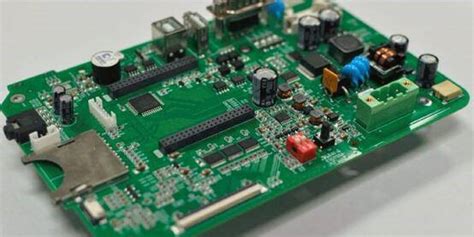
Applications and Production Process of Rigid-Flex PCBs
1.Substrate: FCCL (Flexible Copper Clad Laminate)
Polyamide: Kapton (12.5um/20um/25um/50um/75um): Features good flexibility, high temperature resistance (long-term operating temperature 260°C, short-term resistance 400°C), high moisture absorption, excellent electrical and mechanical properties, and good tear resistance. It also offers good weather and chemical resistance and flame retardancy. Polyester amine (PI) is the most widely used, 80% of which is produced by DuPont in the United States.
Polyester (25um/50um/75um): Inexpensive, offers good flexibility and tear resistance. It also has good mechanical and electrical properties such as tensile strength, as well as good water resistance and moisture absorption. However, it shrinks significantly after heating and has poor high-temperature resistance. It is not suitable for high-temperature soldering, with a melting point of 250°C, and is relatively rarely used today.

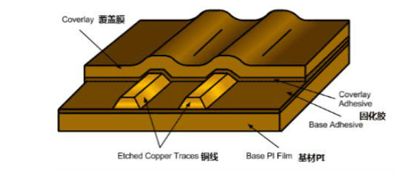
2.Coverlay
The main function of the coverlay is to protect the circuitry from moisture, contamination, and solder resistance.
The coverlay thickness ranges from 1/2 mil to 5 mils (12.7 to 127 μm). The conductive layer (conductive layer) is produced using several methods: rolled copper (rolled annealed copper), electrolytic copper (electrodeposited copper), and silver sputtering/spraying (silver ink). The crystal structure of electrolytic copper is rough, which is not conducive to fine-line yield. The crystal structure of rolled copper is smooth, but the bonding strength with the base film is poor. You can distinguish between rolled copper foil and electrolytic copper foil from the outside.
Electrolytic copper foil is copper-red, while rolled copper foil is off-white. Auxiliary material and reinforcement plate (additional material and reinforcement). A hard material partially pressed onto the flexible PCB to solder components or increase mounting strength.
Reinforcement films can be used for FR4, resin boards, pressure-sensitive adhesives, and steel and aluminum reinforcement. Prepreg sheets (low-flow PP) do not contain flowable or non-flowable adhesives. They are used for laminating flexible and rigid boards (rigid-flexible connections), typically very thin PP.
Typically, 2 mil, 1080 (3.0 mil/3.5 mil), and 2116 (5.6 mil) are used.
3.Rigid and Flexible PCB Structures
Rigid and flexible PCBs bond one or more rigid layers onto a flexible board. The rigid and flexible layers of the circuitry are interconnected through metallization. Each rigid and flexible bonded board has one or more rigid and flexible areas. The following example shows a simple rigid and flexible board combination with multiple layers.

Alternatively, a flexible board is combined with several rigid boards, or several flexible boards are combined with several rigid boards. Electrical interconnection is achieved using drilling, hole coating, and lamination processes. Based on design requirements, tailor the design concept to best suit equipment installation and commissioning, as well as soldering operations. Ensure optimal utilization of the advantages and flexibility of rigid and flexible bonded boards. This situation is more complex when there are more than two layers of wiring. The following are examples:
A composite material is a multilayer board composed of copper foil, P-sheet, memory flexible wiring, and external rigid pressure. Rigid bonded board lamination differs from lamination of only flexible boards or rigid boards. Not only must deformation of the flexible board be considered during lamination, but the surface smoothness of the rigid board must also be considered. Therefore, in addition to material selection, the appropriate thickness of the rigid board must be considered during the design process to ensure consistent shrinkage of the rigid portion and prevent warping. Experimental results have shown that a thickness of 0.8-1.0mm is more suitable.
Also, it is important to ensure that holes in the rigid and flexible boards are spaced a certain distance from the junction to avoid impacting the rigid bonded portion.
4.Rigid and Flexible PCB Production Process
Rigid and flexible bonded boards combine FPC and PCB. Rigid and flexible bonded board production requires both FPC production equipment and PCB processing equipment. First, electronics engineers design the required lines and shapes for the flexible adhesive board. These are then sent to the rigid-flexible board manufacturing plant. After CAM engineers process the relevant documents and conduct planning, the FPC production line is assigned to produce the required FPC, and the PCB production line is assigned to produce the PCB. The two flexible and rigid boards are then produced.
According to the electronics engineers’ planning requirements, the FPC and PCB are seamlessly compacted using a press. After a series of detailed processes, the rigid-flexible boards are finally processed. Considering Motorola’s 1+2F+1 mobile display and side key design, a 4-layer board (two rigid and two flexible) is required. The board design requirements are HDI (High-Definition Interface) with a 0.5mm BGA pitch. The flexible board is 25µm thick and features IVH (Interlayer Via Hole) holes. The overall board thickness is 0.295 ± 0.052mm. The inner layer LW/SP is 3/3 mil.