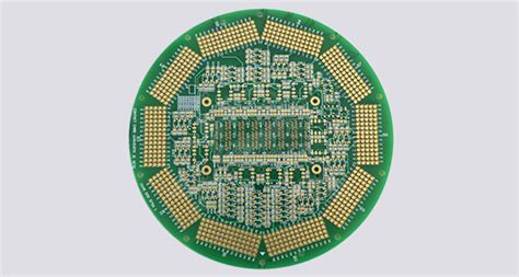
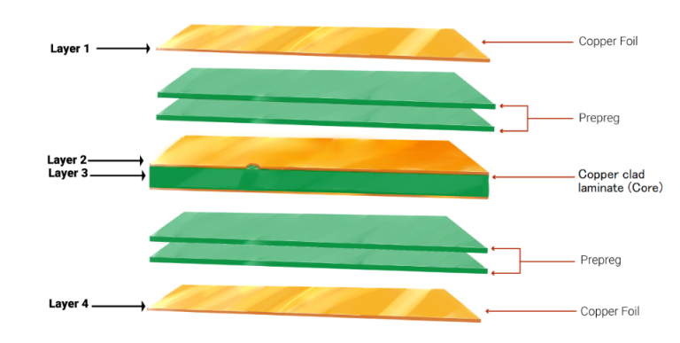
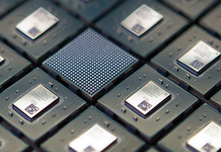
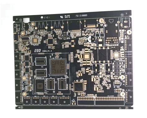
Assembly pcb
Benefits Of Automated PCB Assembly
Automated PCB assembly has revolutionized the electronics manufacturing industry, offering a multitude of benefits that enhance efficiency, accuracy, and overall production quality.
One of the primary advantages of automated PCB assembly is the significant reduction in human error.
Manual assembly processes are inherently prone to mistakes, which can lead to defective products and increased costs. Automation, on the other hand, ensures that each component is placed with precision, thereby minimizing the likelihood of errors and improving the reliability of the final product.
In addition to reducing errors, automated PCB assembly significantly accelerates the production process.
Traditional manual assembly is time-consuming and labor-intensive, often requiring skilled technicians to meticulously place and solder each component. Automation streamlines these tasks, allowing for rapid assembly of complex PCBs. This increased speed not only boosts production capacity but also enables manufacturers to meet tight deadlines and respond swiftly to market demands. Consequently, companies can achieve faster time-to-market for their products, giving them a competitive edge.
Moreover, automated PCB assembly enhances consistency and repeatability in the manufacturing process.
Human operators, no matter how skilled, can introduce variability in the assembly process due to fatigue, distractions, or other factors. Automated systems, however, operate with unwavering consistency, ensuring that each PCB is assembled to the same high standard. This uniformity is particularly crucial for high-volume production runs, where even minor deviations can lead to significant quality issues.
Another notable benefit of automated PCB assembly is the ability to handle increasingly complex designs.
Modern electronic devices often feature intricate and densely packed PCBs, which can be challenging to assemble manually. Automated systems, equipped with advanced placement and soldering technologies, can effortlessly manage these complexities. This capability not only expands the range of possible designs but also allows for greater innovation in product development.
Furthermore, automated PCB assembly contributes to cost savings in several ways.
While the initial investment in automation equipment can be substantial, the long-term savings are considerable. Reduced labor costs, lower error rates, and faster production times all contribute to a more cost-effective manufacturing process. Additionally, automation can lead to better utilization of materials, as precise component placement reduces waste and rework. Over time, these savings can offset the initial investment and result in a more profitable operation.
Environmental considerations also play a role in the benefits of automated PCB assembly.
Automated systems are typically more efficient in their use of energy and materials compared to manual processes. This efficiency translates to a smaller environmental footprint, aligning with the growing emphasis on sustainable manufacturing practices. By reducing waste and optimizing resource use, automated PCB assembly supports the broader goal of environmental responsibility.
In conclusion, the benefits of automated PCB assembly are manifold, encompassing improved accuracy, speed, consistency, and cost-effectiveness. As the electronics industry continues to evolve, the adoption of automation technologies will likely become even more widespread, driving further advancements in manufacturing capabilities. By embracing automated PCB assembly, companies can not only enhance their production processes but also position themselves for long-term success in an increasingly competitive market.
Common Challenges In PCB Assembly And How To Overcome Them
Printed Circuit Board (PCB) assembly is a critical process in the manufacturing of electronic devices, involving the placement and soldering of electronic components onto a PCB. Despite advancements in technology, several challenges persist in PCB assembly, which can impact the quality and functionality of the final product. Understanding these common challenges and implementing effective strategies to overcome them is essential for ensuring the reliability and performance of electronic devices.
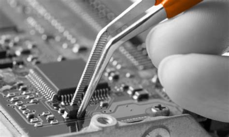
One of the primary challenges in PCB assembly is component placement accuracy.
As electronic devices become more compact and complex, the need for precise placement of components on the PCB becomes increasingly critical. Misalignment or incorrect placement can lead to short circuits, open circuits, or other functional failures.
To address this issue, manufacturers can utilize advanced pick-and-place machines equipped with high-resolution cameras and sophisticated algorithms. These machines can accurately position components, even on densely populated boards, thereby reducing the risk of placement errors.
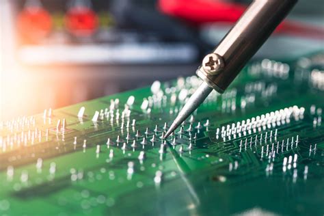
Another significant challenge is soldering defects, which can manifest as solder bridges, cold joints, or insufficient solder.
These defects can compromise the electrical connectivity and mechanical stability of the assembled PCB. To mitigate soldering issues, it is crucial to maintain optimal soldering conditions, including temperature control, solder paste quality, and proper reflow profiles. Implementing automated optical inspection (AOI) systems can also help detect soldering defects early in the assembly process, allowing for timely corrective actions.
Thermal management is another critical aspect of PCB assembly that poses challenges.
As electronic components generate heat during operation, inadequate thermal management can lead to overheating, reduced performance, and even component failure. Effective thermal management strategies include the use of thermal vias, heat sinks, and thermal interface materials to dissipate heat away from critical components. Additionally, designing PCBs with proper thermal considerations, such as adequate spacing between heat-generating components, can enhance heat dissipation and improve overall reliability.
Component availability and supply chain disruptions are also common challenges in PCB assembly.
The global electronics industry is highly dependent on a complex supply chain, and any disruptions can lead to delays in production and increased costs. To mitigate this risk, manufacturers can adopt strategies such as maintaining a diversified supplier base, establishing strong relationships with suppliers, and keeping buffer stock of critical components. Additionally, leveraging supply chain management software can provide real-time visibility into inventory levels and potential disruptions, enabling proactive decision-making.
Furthermore, ensuring the quality and reliability of assembled PCBs requires rigorous testing and inspection processes.
Functional testing, in-circuit testing (ICT), and AOI are essential to identify defects and verify the performance of the assembled PCBs. Implementing a robust quality control system, including statistical process control (SPC) and continuous improvement initiatives, can help identify and address process variations that may lead to defects.
In conclusion, while PCB assembly presents several challenges, adopting advanced technologies and best practices can significantly mitigate these issues. Accurate component placement, effective soldering techniques, robust thermal management, proactive supply chain strategies, and rigorous testing and inspection processes are key to overcoming common challenges in PCB assembly. By addressing these challenges, manufacturers can ensure the production of high-quality, reliable electronic devices that meet the demands of today’s technology-driven world.
Innovations In Surface Mount Technology (SMT) For PCB Assembly
Surface Mount Technology (SMT) has revolutionized the field of Printed Circuit Board (PCB) assembly, offering numerous advantages over traditional through-hole technology. As the demand for smaller, more efficient, and higher-performing electronic devices continues to grow, innovations in SMT have become increasingly critical. These advancements not only enhance the functionality and reliability of electronic products but also streamline the manufacturing process, making it more cost-effective and environmentally friendly.
One of the most significant innovations in SMT is the development of advanced soldering techniques.
Traditional wave soldering methods have been largely supplanted by reflow soldering, which provides greater precision and control. Reflow soldering involves applying solder paste to the PCB, placing the components, and then heating the assembly in a reflow oven. This process ensures that the solder melts and forms reliable connections without damaging sensitive components. Moreover, the introduction of lead-free soldering, driven by environmental regulations such as the Restriction of Hazardous Substances (RoHS) directive, has further refined the reflow soldering process. Lead-free solders typically have higher melting points, necessitating more precise temperature control to avoid thermal stress on components.
In addition to soldering advancements, the miniaturization of components has played a pivotal role in SMT innovation.
The development of smaller, more efficient components, such as microcontrollers, resistors, and capacitors, has enabled the production of compact and lightweight electronic devices. This miniaturization trend is supported by the use of fine-pitch components and ball grid arrays (BGAs), which allow for higher component density on PCBs. Consequently, manufacturers can design more complex circuits within a smaller footprint, enhancing the overall performance and functionality of electronic products.
Another noteworthy innovation in SMT is the implementation of automated assembly processes.
Automation has significantly improved the efficiency and accuracy of PCB assembly, reducing the likelihood of human error and increasing production throughput.
Automated pick-and-place machines, for instance, can rapidly and precisely position components on the PCB, ensuring consistent quality and alignment.
Furthermore, advancements in machine vision technology have enhanced the capability of these machines to detect and correct placement errors in real-time, further improving the reliability of the assembly process.
The integration of advanced inspection and testing methods has also contributed to the evolution of SMT.
Automated optical inspection (AOI) and X-ray inspection systems are now commonly used to verify the quality of solder joints and detect defects that may not be visible to the naked eye. These inspection techniques provide valuable feedback during the assembly process, allowing for immediate corrective actions and reducing the risk of defective products reaching the market. Additionally, in-circuit testing (ICT) and functional testing have become integral parts of the SMT assembly process, ensuring that assembled PCBs meet the required performance specifications before they are deployed in end-use applications.
Moreover, the adoption of advanced materials and substrates has further propelled SMT innovation.
High-performance materials, such as flexible PCBs and high-frequency laminates, offer superior electrical and thermal properties, enabling the development of cutting-edge electronic devices. These materials are particularly beneficial in applications requiring high-speed data transmission and efficient heat dissipation, such as telecommunications and automotive electronics.
In conclusion, the continuous advancements in Surface Mount Technology have significantly transformed PCB assembly, driving the development of more compact, efficient, and reliable electronic devices. Innovations in soldering techniques, component miniaturization, automated assembly processes, inspection methods, and advanced materials have collectively enhanced the capabilities of SMT, meeting the ever-evolving demands of the electronics industry. As technology continues to advance, it is anticipated that SMT will further evolve, paving the way for even more sophisticated and high-performing electronic products.
Quality Control Techniques In PCB Assembly
Quality control is a critical aspect of printed circuit board (PCB) assembly, ensuring that the final product meets the required standards and functions as intended. The process begins with the inspection of raw materials, where components and substrates are scrutinized for any defects or inconsistencies. This initial step is crucial, as the quality of the raw materials directly impacts the overall reliability of the PCB. By employing advanced techniques such as X-ray fluorescence (XRF) analysis, manufacturers can verify the composition of materials, ensuring compliance with industry standards.
Moving forward, the assembly process itself is subject to rigorous quality control measures.
One of the primary techniques used is Automated Optical Inspection (AOI). AOI systems utilize high-resolution cameras to capture detailed images of the PCB, which are then analyzed for defects such as misaligned components, soldering issues, and missing parts. This non-contact method allows for rapid and accurate inspection, significantly reducing the likelihood of human error. Additionally, AOI can be integrated into various stages of the assembly process, providing continuous monitoring and immediate feedback.
In conjunction with AOI, manufacturers often employ Automated X-ray Inspection (AXI) to examine the internal structure of the PCB.
AXI is particularly useful for detecting hidden defects, such as voids in solder joints or misaligned vias, which are not visible through optical inspection alone. By using X-ray technology, AXI provides a comprehensive view of the PCB’s internal features, ensuring that even the most minute defects are identified and addressed.
Another essential quality control technique is In-Circuit Testing (ICT).
ICT involves the use of specialized test fixtures and probes to evaluate the electrical performance of the assembled PCB. This method allows for the detection of issues such as short circuits, open circuits, and incorrect component values. By verifying the electrical functionality of the PCB, ICT ensures that the final product will perform as expected in real-world applications. Furthermore, ICT can be customized to accommodate various PCB designs, making it a versatile and widely adopted technique in the industry.
Functional testing is another critical aspect of quality control in PCB assembly. Unlike ICT, which focuses on individual components and connections, functional testing evaluates the overall performance of the PCB in its intended application. This method involves simulating real-world operating conditions and assessing the PCB’s response to various inputs and outputs. By conducting functional tests, manufacturers can identify potential issues that may not be apparent through other inspection methods, ensuring that the final product meets the required performance standards.
To complement these inspection and testing techniques, manufacturers also implement stringent process controls throughout the assembly process.
Statistical Process Control (SPC) is a widely used method that involves the collection and analysis of data to monitor and control the assembly process. By identifying trends and variations in the data, SPC enables manufacturers to make informed decisions and implement corrective actions as needed. This proactive approach helps to maintain consistent quality and minimize the occurrence of defects.
In addition to these technical measures, effective communication and collaboration among team members play a vital role in ensuring quality control.
By fostering a culture of continuous improvement and encouraging feedback from all levels of the organization, manufacturers can identify and address potential issues more effectively. Regular training and development programs also help to ensure that employees are well-versed in the latest quality control techniques and best practices.
In conclusion, quality control in PCB assembly is a multifaceted process that involves a combination of advanced inspection techniques, rigorous testing methods, and robust process controls. By implementing these measures, manufacturers can ensure that their products meet the highest standards of quality and reliability, ultimately delivering superior performance to end-users.