Automated Optical Inspection (AOI) in PCB Manufacturing: Principles, Applications, and Future Trends
Introduction
Automated Optical Inspection (AOI) has become an indispensable technology in modern Printed Circuit Board (PCB) manufacturing, offering fast, accurate, and reliable quality control throughout the production process. As electronic devices continue to shrink in size while growing in complexity, the need for precise inspection methods has never been greater. AOI systems provide manufacturers with the capability to detect defects early in the production cycle, reducing waste, improving yields, and ensuring product reliability.
This article explores the fundamental principles of AOI technology, its implementation in PCB manufacturing processes, the types of defects it can identify, recent technological advancements, and future trends in this critical field of electronics manufacturing.
Fundamentals of AOI Technology
Basic Working Principles
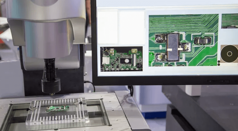
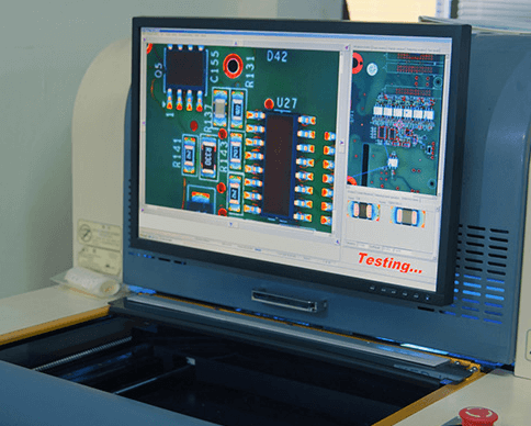
Automated Optical Inspection systems for PCB applications operate on the principle of comparing captured images of manufactured boards against reference standards or design specifications. These systems typically consist of high-resolution cameras, sophisticated lighting systems, precision motion control mechanisms, and powerful image processing software.
The inspection process begins with the system capturing digital images of the PCB under controlled lighting conditions. These images are then analyzed using various algorithms to identify potential defects. The comparison can be made against several references:
- Golden Board Comparison: Using a known-good PCB as the reference standard
- CAD Data Comparison: Comparing against the original design files
- Statistical Modeling: Using accumulated data from previous inspections to establish acceptable parameters
Key Components of AOI Systems
Modern AOI systems incorporate several critical components that work together to ensure accurate inspection:
- Imaging System: High-resolution cameras (often with multiple megapixels) capture detailed images of the PCB. Some systems use line scan cameras for continuous inspection, while others employ area scan cameras for stationary capture.
- Lighting System: Advanced illumination techniques, including bright-field, dark-field, coaxial, and multi-angle lighting, help reveal different types of defects. Many systems use programmable LED arrays that can adjust intensity, angle, and color to optimize defect detection.
- Motion Control: Precision XY tables or robotic arms position the camera and/or PCB to ensure complete coverage. High-end systems can achieve micron-level positioning accuracy.
- Image Processing Hardware: Powerful processors, often with specialized hardware acceleration (such as GPUs or FPGAs), handle the massive computational requirements of real-time image analysis.
- Inspection Software: Sophisticated algorithms perform pattern matching, blob analysis, edge detection, and other image processing techniques to identify potential defects.
AOI in the PCB Manufacturing Process
Placement in the Production Line
AOI systems are strategically placed at multiple points in the PCB manufacturing process to catch defects as early as possible:
- Post-Solder Paste Inspection (SPI): Some lines include AOI immediately after solder paste application to verify stencil printing quality before component placement.
- Pre-Reflow Inspection: After component placement but before reflow soldering, AOI can verify component presence, correct placement, and polarity.
- Post-Reflow Inspection: The most common AOI checkpoint examines the board after soldering to detect soldering defects, component issues, and other assembly problems.
- Final Inspection: A comprehensive check before shipping ensures overall product quality.
Types of Defects Detected
AOI systems can identify a wide range of PCB assembly defects, including but not limited to:
Component-level defects:
- Missing components
- Misaligned or misoriented parts
- Wrong component values or packages
- Lifted or tombstoned components
- Damaged components (cracked, chipped)
Soldering defects:
- Solder bridges (shorts)
- Insufficient solder (opens)
- Excessive solder
- Solder balls or splashes
- Cold solder joints
- Voiding in BGA joints (with X-ray capable systems)
PCB defects:
- Trace damage or cuts
- Solder mask issues
- Contamination or foreign material
- Pad lifting
- Copper foil defects
Advantages of AOI in PCB Manufacturing
The implementation of AOI systems offers numerous benefits to PCB manufacturers:
- Improved Quality Control: AOI provides consistent, objective inspection that surpasses human capabilities for many defect types, especially in high-density assemblies.
- Increased Throughput: Modern AOI systems can inspect boards in seconds, keeping pace with high-speed production lines without becoming a bottleneck.
- Early Defect Detection: By catching problems early in the process, AOI reduces the cost of rework and prevents defective boards from progressing through subsequent production stages.
- Process Optimization: The data collected by AOI systems can be analyzed to identify trends and root causes of defects, enabling continuous process improvement.
- Documentation and Traceability: Automated inspection creates a digital record of each board’s quality status, supporting quality assurance protocols and regulatory compliance.
- Reduced Labor Costs: While not eliminating the need for human operators entirely, AOI significantly reduces the manpower required for visual inspection.
Technological Advancements in AOI
Recent years have seen significant advancements in AOI technology that have expanded its capabilities:
1. 3D AOI Systems
Traditional 2D AOI systems have limitations in measuring solder joint quality, particularly for components like BGAs where the solder joints are hidden. 3D AOI systems use techniques such as:
- Laser triangulation
- Structured light projection
- Stereo vision
These methods provide height information that enables better assessment of solder volume and shape, particularly for through-hole and fine-pitch components.
2. Enhanced Imaging Technologies
New imaging technologies have improved AOI capabilities:
- Higher Resolution Cameras: Modern systems now routinely offer 20+ megapixel resolution for inspecting ultra-fine pitch components.
- Multispectral Imaging: Using different wavelengths of light can reveal defects that are invisible under standard illumination.
- High-Speed Cameras: Enable inspection of moving boards without stopping the production line.
3. Advanced Algorithms and AI
The application of artificial intelligence, particularly deep learning, has revolutionized defect detection:
- Convolutional Neural Networks (CNNs): Can learn to identify defects from examples rather than relying solely on programmed rules.
- Anomaly Detection: Machine learning models can detect subtle, previously undefined defects by learning what “normal” boards look like.
- Reduced False Calls: AI can help distinguish between actual defects and acceptable variations, reducing unnecessary rework.
4. Integration with Other Systems
Modern AOI doesn’t operate in isolation but as part of an interconnected manufacturing ecosystem:
- Integration with SPI and AXI: Combining data from Solder Paste Inspection and Automated X-ray Inspection systems provides a more comprehensive quality picture.
- MES Connectivity: Direct links to Manufacturing Execution Systems enable real-time process adjustments based on inspection results.
- Industry 4.0 Compatibility: Cloud connectivity and data analytics support predictive maintenance and continuous process improvement.
Challenges and Limitations of AOI
Despite its many advantages, AOI technology does face some challenges:
- False Calls: Both false positives (identifying good features as defects) and false negatives (missing actual defects) remain persistent issues, though AI is helping to reduce these.
- Hidden Joints: Traditional AOI cannot inspect hidden solder joints like those in BGA packages, requiring complementary X-ray inspection.
- Programming Complexity: Setting up inspection programs for new board designs can be time-consuming, though template-based and AI-assisted programming is improving this.
- High Initial Investment: Advanced AOI systems represent a significant capital expenditure, though the ROI is typically favorable for medium to high-volume production.
- Maintenance Requirements: Regular calibration and maintenance are needed to maintain optimal performance.
Future Trends in AOI Technology
The field of AOI continues to evolve rapidly. Several key trends are shaping its future development:
- Increased AI Integration: More sophisticated machine learning models will enable “self-learning” inspection systems that improve over time with minimal manual programming.
- Combined Inspection Technologies: Hybrid systems combining AOI with other inspection methods (AXI, ultrasound, thermal imaging) will provide more comprehensive quality assessment.
- Faster Processing Speeds: As electronics continue to miniaturize, AOI systems will need to keep pace with higher resolution and faster inspection requirements.
- Predictive Quality Analytics: By combining inspection data with process parameters, systems will predict and prevent defects before they occur.
- Enhanced User Interfaces: More intuitive programming interfaces and augmented reality tools will make AOI systems easier to set up and operate.
- Adaptive Inspection: Systems that automatically adjust inspection criteria based on real-time process variations and historical defect patterns.
Conclusion
Automated Optical Inspection has become a cornerstone technology in modern PCB manufacturing, essential for maintaining quality in an era of increasingly complex and miniaturized electronics. From its basic principles of optical comparison to the latest advancements in artificial intelligence and 3D imaging, AOI continues to evolve to meet the challenges of electronics manufacturing.
As the technology progresses, we can expect AOI systems to become even more intelligent, integrated, and indispensable. The future of AOI lies not just in detecting defects, but in preventing them through predictive analytics and closed-loop process control. For PCB manufacturers looking to maintain competitiveness in quality, yield, and efficiency, investment in advanced AOI technology is not just an option—it’s a necessity.
The continued development of AOI will play a crucial role in enabling next-generation electronics, from 5G devices to IoT products and beyond, ensuring that the foundation of our digital world—the printed circuit board—meets ever-higher standards of reliability and performance