Autonomous Driving PCB: Design, Challenges, and Future Trends
1. Introduction
The rapid advancement of autonomous driving technology has revolutionized the automotive industry. At the heart of this transformation lies the Printed Circuit Board (PCB), which serves as the foundation for the complex electronic systems enabling self-driving capabilities. Autonomous driving PCBs integrate high-performance computing, sensor interfaces, power management, and communication modules to ensure safe and efficient vehicle operation.
This article explores the key aspects of autonomous driving PCBs, including their design requirements, challenges, materials, and future trends.
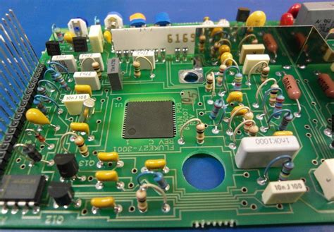
2. Key Components of Autonomous Driving PCBs
Autonomous vehicles rely on multiple subsystems, each requiring specialized PCB designs. The primary components include:
2.1. Central Processing Unit (CPU) and AI Accelerators
Modern autonomous vehicles use powerful processors, such as NVIDIA’s Drive platform or Mobileye’s EyeQ chips, to process vast amounts of sensor data in real time. These high-performance computing modules require:
- High-density interconnects (HDI) for efficient signal routing.
- Advanced thermal management to dissipate heat from high-power chips.
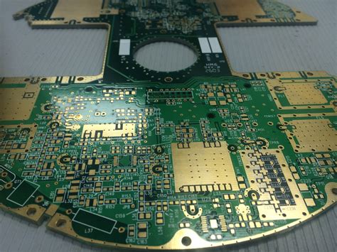
- Multi-layer PCBs (12+ layers) to accommodate complex circuitry.
2.2. Sensor Interfaces
Autonomous vehicles depend on multiple sensors, including:
- LiDAR (Light Detection and Ranging) – Requires high-frequency PCBs for precise signal integrity.
- Radar (Radio Detection and Ranging) – Uses RF PCB designs with controlled impedance.
- Cameras – High-speed interfaces (e.g., MIPI CSI-2) demand low-latency signal transmission.
- Ultrasonic Sensors – Simpler PCB layouts but require noise immunity.
2.3. Vehicle Communication Modules
- V2X (Vehicle-to-Everything) Communication – Uses 5G and DSRC (Dedicated Short-Range Communication) PCBs with RF optimization.
- CAN (Controller Area Network) & Automotive Ethernet – High-reliability PCBs for in-vehicle networking.
2.4. Power Management Systems
- High-current PCBs for battery management systems (BMS).
- Voltage regulation circuits to ensure stable power delivery.
3. Design Challenges for Autonomous Driving PCBs
Designing PCBs for autonomous vehicles presents several challenges:
3.1. Signal Integrity and EMI Control
- High-speed signals (e.g., from LiDAR and cameras) require controlled impedance traces and proper grounding techniques.
- EMI (Electromagnetic Interference) must be minimized to prevent sensor malfunctions.
3.2. Thermal Management
- High-power processors generate significant heat, necessitating thermal vias, heat sinks, and metal-core PCBs.
- Liquid cooling solutions may be integrated into advanced designs.
3.3. Reliability in Harsh Environments
- Autonomous driving PCBs must withstand temperature extremes, vibrations, and moisture.
- Conformal coating and robust material selection (e.g., high-Tg laminates) enhance durability.
3.4. Miniaturization and High-Density Layouts
- With increasing functionality, PCBs must fit into compact spaces while maintaining performance.
- HDI (High-Density Interconnect) technology and microvias enable tighter routing.
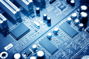
4. Material Selection for Autonomous Driving PCBs
The choice of PCB materials significantly impacts performance:
4.1. High-Frequency Materials
- Rogers RO4000 series – Used for RF and millimeter-wave applications (e.g., radar).
- PTFE (Teflon)-based laminates – Provide low dielectric loss for high-speed signals.
4.2. High-Temperature Materials
- FR-4 with high Tg (Glass Transition Temperature >170°C) – Ensures stability under thermal stress.
- Ceramic-filled substrates – Improve heat dissipation.
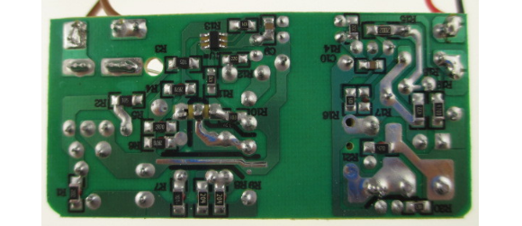
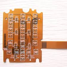
4.3. Flexible and Rigid-Flex PCBs
- Used in compact sensor modules and wiring harnesses.
- Polyimide-based flex PCBs offer durability in dynamic environments.
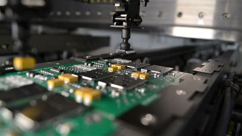
5. Manufacturing and Testing Considerations
5.1. Advanced Manufacturing Techniques
- Laser drilling for microvias in HDI PCBs.
- Automated Optical Inspection (AOI) to detect soldering defects.
- 3D printing for rapid prototyping of complex PCB designs.
5.2. Rigorous Testing Protocols
- Automated Test Equipment (ATE) for functional validation.
- Environmental stress testing (thermal cycling, vibration tests) to ensure reliability.
- Signal integrity analysis using TDR (Time Domain Reflectometry).
6. Future Trends in Autonomous Driving PCBs
6.1. Integration of AI-Optimized Hardware
- Neuromorphic computing chips may replace traditional CPUs for faster AI processing.
- In-memory computing PCBs could reduce latency in decision-making.
6.2. Adoption of 5G and V2X Technologies
- Higher-frequency PCBs (mmWave) for ultra-low-latency communication.
- Antenna-embedded PCBs for seamless V2X integration.
6.3. Sustainable and Lightweight PCB Materials
- Bio-based resins for eco-friendly PCBs.
- Carbon fiber-reinforced substrates to reduce weight.
6.4. Autonomous Vehicle-Specific Standards
- ISO 26262 compliance for functional safety.
- AEC-Q100 qualified components for automotive-grade reliability.
7. Conclusion
Autonomous driving PCBs are at the core of next-generation vehicles, enabling advanced perception, decision-making, and control. Their design involves overcoming challenges related to signal integrity, thermal management, and reliability while leveraging cutting-edge materials and manufacturing techniques.
As autonomous technology evolves, PCBs will continue to advance, incorporating AI acceleration, 5G connectivity, and sustainable materials. The future of autonomous driving depends on innovations in PCB technology, making it a critical area of research and development in the automotive industry.
By addressing these challenges and embracing emerging trends, engineers can develop robust PCBs that power the self-driving cars of tomorrow.