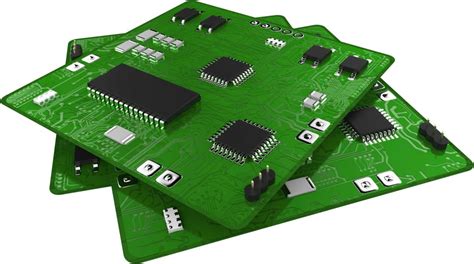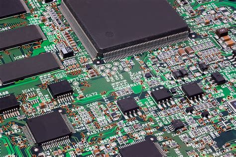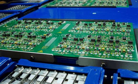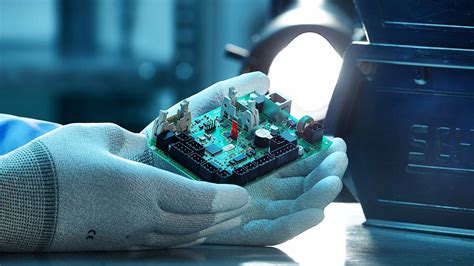
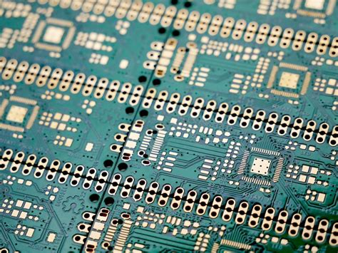
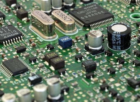
Bare die pcb assembly
Advantages Of Bare Die PCB Assembly In Modern Electronics
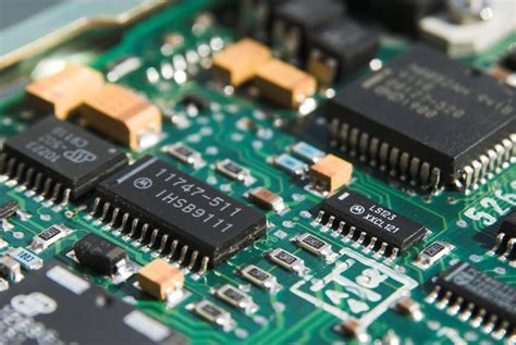
Bare die PCB assembly, a sophisticated technique in the realm of modern electronics, offers a multitude of advantages that are increasingly being recognized by engineers and manufacturers alike.
This method involves mounting unpackaged semiconductor chips directly onto a printed circuit board (PCB), which can lead to significant improvements in performance, size, and cost-effectiveness. As the demand for more compact and efficient electronic devices continues to grow, the benefits of bare die PCB assembly become ever more pertinent.
One of the primary advantages of bare die PCB assembly is the reduction in size and weight of electronic devices.
By eliminating the need for individual chip packaging, this method allows for a more compact design. This is particularly beneficial in applications where space is at a premium, such as in mobile devices, wearable technology, and aerospace systems. The ability to place chips closer together on the PCB not only saves space but also reduces the overall weight of the device, which is a critical factor in portable and airborne applications.
In addition to size and weight reduction, bare die PCB assembly can enhance the performance of electronic devices.
The direct mounting of chips onto the PCB minimizes the parasitic inductance and capacitance that are often introduced by traditional packaging. This results in improved electrical performance, including faster signal transmission and reduced power consumption. Consequently, devices assembled using this technique can operate more efficiently and with greater speed, which is a significant advantage in high-performance computing and telecommunications.
Moreover, bare die PCB assembly can lead to cost savings in the manufacturing process.
By bypassing the need for individual chip packaging, manufacturers can reduce material costs and simplify the assembly process. This can result in lower production costs, which can be particularly advantageous in high-volume manufacturing scenarios. Furthermore, the streamlined assembly process can lead to shorter production times, allowing manufacturers to bring products to market more quickly and respond more agilely to changes in consumer demand.
Another noteworthy benefit of bare die PCB assembly is the potential for improved thermal management.
The direct attachment of chips to the PCB allows for more efficient heat dissipation, as there are fewer barriers to impede the transfer of heat away from the chip. This can be particularly important in high-power applications where effective thermal management is crucial to maintaining device reliability and longevity. By enhancing heat dissipation, bare die PCB assembly can help prevent overheating and extend the lifespan of electronic components.
Despite these advantages, it is important to acknowledge that bare die PCB assembly also presents certain challenges.
The process requires precise handling and placement of delicate semiconductor chips, which can necessitate specialized equipment and expertise. Additionally, the lack of protective packaging means that chips are more exposed to environmental factors, potentially increasing the risk of damage. However, advancements in technology and materials are continually addressing these challenges, making bare die PCB assembly an increasingly viable option for a wide range of applications.
In conclusion, the advantages of bare die PCB assembly in modern electronics are manifold, encompassing size and weight reduction, enhanced performance, cost savings, and improved thermal management. As technology continues to evolve and the demand for more efficient and compact devices grows, the adoption of this assembly technique is likely to expand, offering new opportunities for innovation and advancement in the electronics industry.
Challenges And Solutions In Bare Die PCB Assembly
Bare die PCB assembly presents a unique set of challenges and opportunities in the field of electronics manufacturing. As the demand for miniaturization and enhanced performance in electronic devices continues to grow, the use of bare die technology has become increasingly prevalent. However, this approach is not without its complexities. Understanding these challenges and exploring potential solutions is crucial for manufacturers aiming to leverage the benefits of bare die PCB assembly.
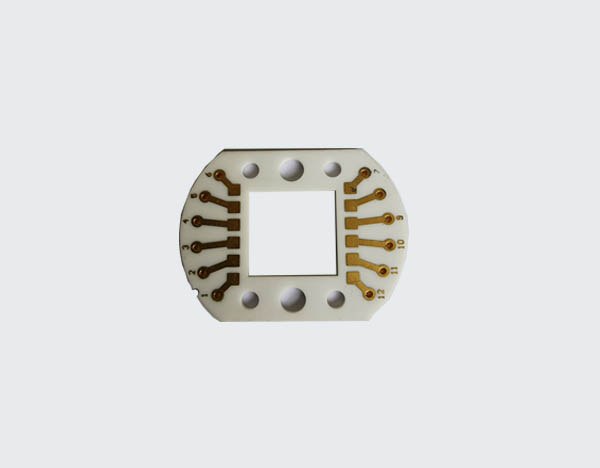
One of the primary challenges in bare die PCB assembly is the handling and placement of the bare die itself.
Unlike packaged components, bare dies are extremely delicate and susceptible to damage from mechanical stress, electrostatic discharge, and contamination. To address this, manufacturers must implement stringent handling protocols and invest in specialized equipment designed to minimize the risk of damage. For instance, the use of advanced pick-and-place machines with high precision and gentle handling capabilities is essential to ensure accurate placement without compromising the integrity of the die.
In addition to handling concerns, the attachment of bare dies to the PCB substrate poses another significant challenge.
Traditional soldering techniques are often unsuitable for bare die assembly due to the absence of a protective package. Instead, manufacturers typically employ techniques such as flip-chip bonding or wire bonding. Flip-chip bonding involves directly attaching the die to the substrate using solder bumps, which provides a robust electrical connection and excellent thermal performance. On the other hand, wire bonding uses fine wires to connect the die to the substrate, offering flexibility in design but requiring meticulous attention to detail to ensure reliability.
Thermal management is another critical consideration in bare die PCB assembly.
As electronic devices become more compact, the heat generated by densely packed components can lead to performance degradation or even failure. To mitigate this, manufacturers must incorporate effective thermal management solutions into their designs. This may involve the use of thermal interface materials, heat sinks, or advanced cooling techniques to dissipate heat efficiently and maintain optimal operating temperatures.
Moreover, the inspection and testing of bare die assemblies present unique challenges.
Traditional inspection methods may not be sufficient to detect defects at the microscopic level required for bare die technology. Consequently, manufacturers often rely on advanced imaging techniques such as X-ray inspection and scanning electron microscopy to identify potential issues. Additionally, rigorous testing protocols must be implemented to ensure the functionality and reliability of the assembled product. This may include electrical testing, thermal cycling, and environmental stress testing to simulate real-world conditions and verify performance.
Despite these challenges, the benefits of bare die PCB assembly are significant.
The elimination of packaging allows for greater design flexibility, reduced size and weight, and improved electrical performance. Furthermore, the ability to integrate multiple dies on a single substrate can lead to enhanced functionality and cost savings. As a result, many industries, including telecommunications, automotive, and consumer electronics, are increasingly adopting bare die technology to meet the demands of modern applications.
In conclusion, while bare die PCB assembly presents a range of challenges, careful consideration and implementation of appropriate solutions can enable manufacturers to harness its advantages effectively. By addressing issues related to handling, attachment, thermal management, and inspection, manufacturers can produce reliable and high-performance electronic devices that meet the evolving needs of the market. As technology continues to advance, the role of bare die PCB assembly is likely to expand, offering exciting possibilities for innovation and development in the electronics industry.
Innovations In Bare Die PCB Assembly Techniques
Bare die PCB assembly has emerged as a pivotal innovation in the electronics manufacturing industry, offering significant advantages in terms of miniaturization, performance, and cost-effectiveness. As the demand for smaller, more efficient electronic devices continues to grow, the need for advanced assembly techniques becomes increasingly critical. Bare die assembly, which involves mounting unpackaged semiconductor dies directly onto a printed circuit board (PCB), is at the forefront of this technological evolution.
One of the primary innovations in bare die PCB assembly is the development of advanced interconnection methods.
Traditional wire bonding, while still in use, is gradually being supplemented and, in some cases, replaced by flip-chip technology. Flip-chip assembly involves placing the die face down on the PCB, allowing for a direct electrical connection through solder bumps. This method not only reduces the overall footprint of the assembly but also enhances electrical performance by minimizing parasitic inductance and resistance. Consequently, flip-chip technology is particularly advantageous in high-frequency applications where signal integrity is paramount.
In addition to interconnection advancements, the materials used in bare die PCB assembly have also seen significant improvements.
The introduction of advanced underfill materials, for instance, has played a crucial role in enhancing the reliability and thermal performance of flip-chip assemblies. Underfill materials are used to fill the gap between the die and the substrate, providing mechanical support and improving thermal conductivity. This innovation is essential for ensuring the longevity and durability of electronic devices, especially those subjected to harsh environmental conditions.
Moreover, the integration of bare die assembly with advanced substrate technologies has further propelled the capabilities of modern electronic devices.
High-density interconnect (HDI) substrates, for example, allow for more complex routing and increased component density, which are essential for the miniaturization of electronic products. By combining bare die assembly with HDI substrates, manufacturers can achieve unprecedented levels of integration and functionality, paving the way for the next generation of compact and powerful electronic devices.
Another noteworthy innovation in bare die PCB assembly is the adoption of advanced inspection and testing techniques.
As the complexity of assemblies increases, ensuring the quality and reliability of each component becomes more challenging. To address this, manufacturers are increasingly relying on automated optical inspection (AOI) and X-ray inspection systems. These technologies enable the detection of defects and anomalies at various stages of the assembly process, ensuring that only high-quality products reach the market. Furthermore, advancements in testing methodologies, such as boundary scan and built-in self-test (BIST), have enhanced the ability to verify the functionality of complex assemblies without the need for physical test probes.
In conclusion, the innovations in bare die PCB assembly techniques are driving significant advancements in the electronics industry. Through the development of advanced interconnection methods, improved materials, and cutting-edge inspection technologies, manufacturers are able to produce smaller, more efficient, and highly reliable electronic devices. As these techniques continue to evolve, they will undoubtedly play a crucial role in shaping the future of electronics, meeting the ever-growing demands for performance and miniaturization. The ongoing research and development in this field promise to unlock new possibilities, further pushing the boundaries of what is achievable in electronic design and manufacturing.
Cost-Effectiveness Of Bare Die PCB Assembly For High-Volume Production
In the realm of electronics manufacturing, the pursuit of cost-effective solutions is a constant endeavor, particularly in high-volume production scenarios. One such solution that has garnered attention is bare die PCB assembly. This method involves mounting unpackaged semiconductor dies directly onto printed circuit boards (PCBs), bypassing the traditional packaging process. The cost-effectiveness of this approach becomes evident when considering several key factors that influence manufacturing expenses.
To begin with, the elimination of the packaging step in bare die PCB assembly significantly reduces material costs.
Traditional semiconductor packaging involves encapsulating the die in a protective casing, which not only adds to the material expenses but also requires additional manufacturing steps. By directly mounting the bare die onto the PCB, manufacturers can avoid these costs, thereby achieving substantial savings. Moreover, the reduction in material usage aligns with sustainable manufacturing practices, which are increasingly prioritized in today’s environmentally conscious market.
In addition to material savings, bare die PCB assembly offers advantages in terms of space efficiency.
The absence of packaging allows for a more compact design, enabling the integration of more components within a given area. This is particularly beneficial in high-volume production, where maximizing the use of available space can lead to significant cost reductions. Furthermore, the compact design can enhance the performance of electronic devices by minimizing signal path lengths, thereby reducing latency and improving overall efficiency.
Another aspect contributing to the cost-effectiveness of bare die PCB assembly is the potential for improved thermal management.
Without the insulating effects of packaging, heat dissipation can be more effectively managed, which is crucial in high-performance applications. Enhanced thermal management not only improves the reliability and longevity of electronic components but also reduces the need for additional cooling solutions, thereby lowering production costs.
Transitioning to the manufacturing process itself, bare die PCB assembly can streamline production workflows.
The direct mounting of dies onto PCBs can simplify assembly lines, reducing the complexity and time required for production. This efficiency is particularly advantageous in high-volume scenarios, where time savings can translate into significant cost reductions. Additionally, the simplified process can lead to lower labor costs, as fewer specialized skills are required compared to traditional packaging and assembly methods.
However, it is important to acknowledge the challenges associated with bare die PCB assembly.
The process requires precise handling and placement of delicate semiconductor dies, necessitating advanced equipment and expertise. While the initial investment in such technology may be substantial, the long-term cost benefits in high-volume production can outweigh these initial expenses. Moreover, advancements in automation and robotics are continually improving the feasibility and cost-effectiveness of bare die assembly, making it an increasingly viable option for manufacturers.
In conclusion, the cost-effectiveness of bare die PCB assembly in high-volume production is underscored by several factors, including reduced material costs, space efficiency, improved thermal management, and streamlined manufacturing processes. While challenges exist, particularly in terms of initial investment and technical expertise, the long-term benefits make it a compelling choice for manufacturers seeking to optimize their production costs. As technology continues to evolve, the adoption of bare die PCB assembly is likely to increase, further solidifying its role as a cost-effective solution in the electronics manufacturing industry.