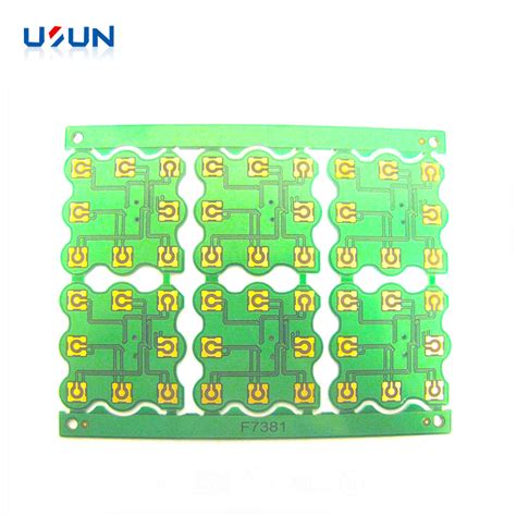
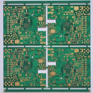
Bare PCB Design: Streamlining Layout and Power Management

Key Takeaways
When designing bare PCBs, you’ll need to balance technical precision with PCB manufacturing cost considerations. Start by understanding how copper layer thickness and stackup configurations influence power delivery—thicker copper reduces resistance but increases material expenses. Partnering with experienced PCB manufacturing companies ensures your layout aligns with production capabilities, avoiding issues like uneven etching or impedance mismatches.
Optimizing component placement requires analyzing thermal pathways and signal return paths. For example, clustering high-power components near voltage regulators minimizes trace lengths, while strategic ground plane segmentation prevents noise coupling. Below is a comparison of common design choices and their manufacturing impacts:
| Design Element | Impact on Manufacturing | Cost Considerations |
|---|---|---|
| Copper Layer Thickness | Higher current handling | Increased PCB manufacturing cost |
| Component Density | Requires advanced assembly tools | Higher per-board expenses |
| Strapping Pin Configuration | Reduces rework risks | Optimizes PCB manufacturing business ROI |
Proper management of strapping pins ensures reliable connections between power domains, particularly in multi-voltage designs. Always validate layouts through simulation tools before finalizing—this step helps avoid costly revisions during prototyping. By integrating these practices, you’ll streamline both performance and PCB manufacturing workflows, delivering boards that meet technical and budgetary targets.

Bare PCB Power Distribution Essentials
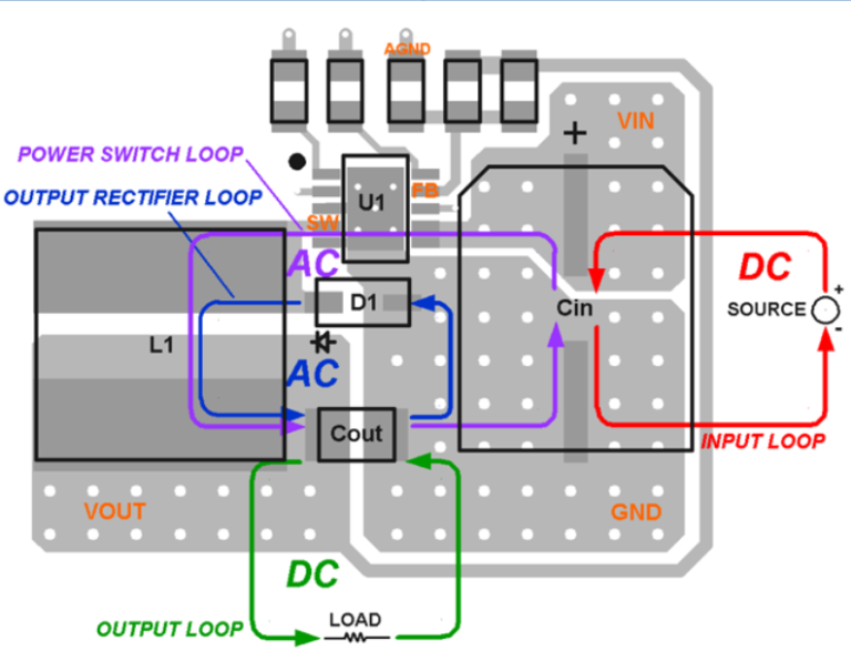
When designing power distribution networks for bare PCBs, you must prioritize efficient current delivery while minimizing voltage drops and electromagnetic interference. Start by evaluating current density requirements across different board sections—this determines copper weight selection and trace widths. Most pcb manufacturing companies recommend using dedicated power planes in multilayer designs to reduce impedance, though this impacts pcb manufacturing cost due to added material layers.
For optimal performance, balance copper thickness with thermal management needs. Thicker traces handle higher currents but increase board weight, affecting compatibility with compact enclosures. A > Tip: "Always simulate power integrity during layout—tools like SPICE models help identify hotspots before prototyping."
Strategic placement of decoupling capacitors near high-power components stabilizes voltage fluctuations, while avoiding parallel routing of power and signal traces prevents crosstalk. When working with pcb manufacturing partners, clarify their capabilities in handling buried vias or asymmetric stackups, which can enhance power delivery in dense layouts.
Don’t overlook strapping pins—these provide secondary connections for critical power paths. Properly managing them reduces reliance on external jumpers, streamlining assembly in high-volume pcb manufacturing business operations. For deeper insights on balancing performance and budget, explore industry-standard power distribution guidelines.
By aligning your design choices with pcb manufacturing realities, you ensure reliable power networks without exceeding cost thresholds or compromising thermal margins.

Copper Layer Configuration Strategies
When designing bare PCBs, your approach to copper layer configuration directly impacts current capacity and thermal dissipation. Start by determining the optimal number of layers based on power requirements: high-current designs often demand thicker copper (2 oz/ft² or higher) for inner planes, while signal layers can use standard 1 oz/ft². PCB manufacturing companies typically recommend separating power and ground planes to minimize noise coupling, but this must align with your PCB manufacturing cost constraints.
For multi-rail systems, dedicate specific layers to distinct voltage domains, ensuring adequate spacing between high-voltage and low-voltage regions. Use cross-hatching in less critical areas to reduce material usage without compromising structural integrity—a tactic that balances performance and PCB manufacturing business economics. When stacking layers, maintain symmetry to prevent warping during fabrication, especially in designs exceeding four layers.
Prioritize continuous copper pours for ground planes to enhance EMI shielding, but avoid creating unintended antennas by isolating high-frequency sections. Collaborate with your PCB manufacturing partner to validate thermal relief patterns around vias, as improper designs risk solder voids during assembly. Remember: even minor adjustments in copper distribution can yield significant improvements in power delivery efficiency, making this phase critical for both functionality and cost optimization.
Component Placement Optimization Techniques
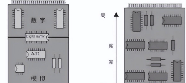
Strategic component placement begins by analyzing power delivery networks and thermal requirements. Start by positioning high-power components near voltage regulators to minimize resistive losses, ensuring PCB manufacturing processes can maintain consistent trace widths for current handling. Group analog and digital sections separately, maintaining at least 3-5mm clearance to reduce electromagnetic interference—a critical consideration for PCB manufacturing companies aiming to meet signal integrity standards.
Next, prioritize thermal-vulnerable parts like ICs or power transistors in airflow-accessible zones, balancing heat distribution across layers. This reduces hotspots that could escalate PCB manufacturing cost through additional cooling solutions. For mixed-signal designs, place decoupling capacitors as close as possible to power pins, creating localized charge reservoirs that stabilize voltage during transient loads.
When arranging connectors or interfaces, align them with board edges to simplify routing and avoid obstructing internal traces. This spatial efficiency directly impacts PCB manufacturing business timelines by reducing redesign iterations. Use automated placement tools to validate clearances and optimize routing paths, but always review critical placements manually to account for thermal expansion or mechanical stress.
Finally, consider testability during layout—ensure probe points and debug headers remain accessible without compromising signal paths. A well-organized placement strategy not only enhances performance but also streamlines assembly, lowering long-term production risks.
Strapping Pin Management Solutions
When addressing strapping pin configurations in PCB manufacturing, precise management becomes critical for maintaining signal integrity and power stability. These pins determine hardware settings through voltage levels or pull-up/down resistors, requiring careful routing to avoid cross-talk or ground bounce. Start by grouping strapping pins near their associated ICs to minimize trace lengths—this reduces impedance variations that could trigger erroneous device states.
Leading PCB manufacturing companies often recommend implementing guard traces or ground shielding between sensitive strapping lines and high-speed signals. For multi-voltage designs, verify resistor networks match your power domains to prevent leakage currents from affecting configuration accuracy. Automated design rule checks (DRCs) can flag insufficient clearance between strapping pins and adjacent components, a common oversight impacting PCB manufacturing cost due to rework.
If your design incorporates programmable logic, ensure strapping pin states remain stable during power sequencing. Pairing weak pull-up resistors with robust decoupling capacitors mitigates voltage fluctuations during startup. For high-volume production, collaborate with PCB manufacturing business partners to validate pin tolerances against process variations—etching inconsistencies or material shifts can alter resistance values, leading to field failures.
By prioritizing these strategies, you balance functional reliability with manufacturability, avoiding costly revisions while maintaining design intent across production batches.

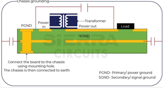
Ground Plane Design Best Practices
When designing ground planes for bare PCBs, prioritize creating a continuous, low-impedance path to minimize noise and stabilize voltage references. Start by dedicating an entire copper layer to the ground plane, as fragmented designs increase electromagnetic interference (EMI) risks. For multi-layer boards, sandwich power and signal layers between ground planes to enhance shielding—a strategy often employed by leading PCB manufacturing companies to balance performance and PCB manufacturing cost.
Avoid splitting the ground plane unnecessarily, but if isolation between analog and digital sections is required, use strategic partitioning with controlled gaps. Always ensure return paths for high-speed signals remain uninterrupted, as abrupt discontinuities can degrade signal integrity. When connecting components, place decoupling capacitors close to power pins and route vias directly to the ground plane—this reduces loop inductance and improves thermal dissipation.
For PCB manufacturing business efficiency, validate your ground plane layout through simulation tools to detect potential hotspots or current crowding. Remember that inadequate grounding in high-frequency designs often leads to rework, inflating production timelines. By aligning your ground plane strategy with industry-standard stack-up configurations, you’ll streamline both performance and scalability across prototyping and mass production phases.
Thermal Management in Bare PCBs
Effective thermal management begins with understanding how heat propagates across bare PCB layers during operation. Critical components like voltage regulators or high-power ICs generate concentrated heat, requiring strategic placement away from thermally sensitive areas. You’ll want to optimize copper layer configurations—thicker copper pours act as heat sinks, while thermal vias transfer heat between layers. However, balancing this with pcb manufacturing cost constraints demands careful planning, as excessive copper or complex via patterns increase material and fabrication expenses.
When designing for heat dissipation, prioritize low-thermal-resistance paths by aligning high-power traces with ground planes. Pcb manufacturing companies often recommend using thermally conductive substrates (like FR-4 with enhanced thermal properties) for applications demanding rigorous thermal performance. For instance, staggered component placement reduces localized hotspots, but this must align with signal integrity layout guidelines to avoid interference.
A common oversight involves neglecting airflow dynamics in the final assembly. Even in bare PCBs, leaving adequate spacing between heat-generating components ensures passive cooling efficiency. Additionally, consult your pcb manufacturing business partner early to validate thermal relief patterns in copper pours, which prevent solder joint stress during reflow. By integrating these practices, you mitigate risks of warping or delamination—issues that escalate long-term pcb manufacturing maintenance costs.
Signal Integrity Layout Guidelines
Maintaining signal integrity requires deliberate planning of trace routing and precise impedance control. Start by minimizing parallel trace lengths between high-speed signals to reduce crosstalk, particularly in dense layouts common in modern pcb manufacturing. Use differential pair routing for critical interfaces, ensuring matched lengths and symmetrical spacing to preserve timing relationships. When implementing ground planes, avoid splitting them beneath high-frequency traces, as discontinuities can introduce unwanted noise or reflections.
For optimal performance, calculate trace widths based on target impedance values early in the design phase. Most pcb manufacturing companies leverage impedance calculators or field solvers to verify these parameters, which directly influence pcb manufacturing cost due to material selection and layer stackup adjustments. Route sensitive signals away from power planes and noisy components like switching regulators, prioritizing shorter paths to reduce susceptibility to electromagnetic interference (EMI).
Incorporate strategic via placement to maintain reference plane continuity, especially when transitioning between layers. If your design involves high-speed connectors or memory interfaces, consult your pcb manufacturing business partner to validate stackup compatibility with signal rise times. Finally, perform post-layout simulations to identify resonance points or impedance mismatches, addressing them before prototyping to avoid costly revisions.
Bare Board Testing Methodology Insights
Effective testing protocols form the backbone of reliable PCB manufacturing, ensuring designs meet functional and quality benchmarks before entering production. When implementing automated optical inspection (AOI) or electrical continuity testing, you’ll need to verify trace integrity and isolate defects like micro-shorts or open circuits. PCB manufacturing companies often prioritize in-circuit testing (ICT) for high-density layouts, as it validates connections between critical nodes while flagging impedance mismatches.
To balance PCB manufacturing cost and precision, consider combining boundary scan techniques with thermal stress testing—this approach identifies latent flaws in copper layers without overextending resources. For multilayer boards, time-domain reflectometry helps assess signal path consistency, particularly when addressing challenges highlighted in earlier sections like ground plane stability.
Your testing strategy should align with the design’s complexity: simpler layouts might rely on flying probe tests, whereas advanced designs demand synchronized validation of power distribution networks. By integrating these methodologies early, PCB manufacturing business workflows minimize rework cycles and uphold signal integrity standards—key factors in sustaining competitive edge across prototyping and mass production phases.
Conclusion
As you finalize your bare PCB design, remember that effective layout and power management require balancing technical precision with practical manufacturing considerations. The choices you make in copper layer configurations and strapping pin arrangements directly influence pcb manufacturing cost and production timelines, especially when collaborating with specialized pcb manufacturing companies. Prioritizing thermal dissipation pathways and signal integrity zones ensures your design aligns with industry standards while maintaining scalability for future iterations in the pcb manufacturing business.
When optimizing component placement, always verify that your grounding strategies complement the pcb manufacturing process—improper alignment can lead to costly reworks. Testing protocols should account for voltage drop scenarios and current leakage risks, particularly in high-density layouts where margins for error shrink. By integrating these principles early, you create boards that not only meet functional requirements but also streamline assembly workflows, reducing bottlenecks for pcb manufacturing partners. Ultimately, a well-executed design bridges the gap between theoretical performance and manufacturable reality, delivering reliability without compromising efficiency.
Frequently Asked Questions
How does component placement affect thermal performance in bare PCBs?
Strategic placement of heat-sensitive components away from high-power elements reduces thermal stress. Working with experienced pcb manufacturing companies ensures proper spacing and airflow considerations are integrated during layout design.
What drives cost variations in pcb manufacturing?
Factors like layer count, material grade, and trace complexity directly impact pcb manufacturing cost. Optimizing copper layer usage and minimizing via counts can lower expenses without compromising performance.
Why prioritize ground plane design in power management?
A continuous ground plane reduces electromagnetic interference (EMI) and stabilizes voltage distribution. This is critical for pcb manufacturing business models focused on high-reliability applications like industrial controls.
How do strapping pins influence signal integrity?
Improper strapping pin configurations create impedance mismatches, leading to signal reflections. Partnering with pcb manufacturing experts ensures pin groupings align with current-carrying requirements and routing constraints.
What testing methods validate bare board reliability?
Automated optical inspection (AOI) and electrical continuity tests are standard. Reputable pcb manufacturing companies combine these with thermal stress tests to identify latent defects before assembly.
Ready to Optimize Your PCB Design?
For tailored solutions in pcb manufacturing, including cost-effective prototyping and high-volume production, please click here to explore advanced design support and manufacturing expertise.