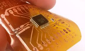
Basic knowledge of soft boards
With the continuous increase in the production ratio of soft PCBs and the application and promotion of rigid-flex PCBs,
it is now more common to add soft, rigid or rigid-flex when talking about PCBs and then say how many layers it is. Usually, PCBs made of soft insulating substrates are called soft PCBs or flexible PCBs, and rigid-flex composite PCBs are called rigid-flex PCBs. It adapts to the needs of today’s electronic products to develop in the direction of high density and high reliability, miniaturization, and lightweight, and also meets strict economic requirements and the needs of market and technological competition.
In foreign countries, soft PCBs have been widely used in the early 1960s. In my country, production and application began in the mid-1960s.
In recent years, with the promotion of global economic integration and the introduction of technology in the open market, its use has continued to grow. Some small and medium-sized rigid PCB factories have seized this opportunity to adopt soft-hard processes, use existing equipment to improve tooling tools and processes, and transform to produce soft PCBs and adapt to the growing demand for soft PCBs. In order to further understand PCBs, here is an exploratory introduction to the soft PCB process.
1.Classification of soft PCBs and their advantages and disadvantages
Classification of flexible PCBs
Flexible PCBs are usually classified as follows based on the number of conductor layers and structure:
1.1 Single-sided flexible PCBs
Single-sided flexible PCBs have only one conductor layer, and the surface may or may not have a covering layer. The insulating substrate material used varies with the application of the product. Commonly used insulating materials include polyester, polyimide, polytetrafluoroethylene, soft epoxy-glass cloth, etc.
Single-sided flexible PCBs can be further divided into the following four categories:
1) Single-sided connection without covering layer
The conductor pattern of this type of flexible PCB is on the insulating substrate, and there is no covering layer on the surface of the conductor. Like the usual single-sided rigid PCB. This type of product is the cheapest one and is usually used in non-critical and environmentally protected applications. Its interconnection is achieved by soldering, fusion welding or pressure welding. It is often used in early telephones.
2) Single-sided connection with covering layer
Compared with the previous type, this type only has an additional covering layer on the surface of the conductor according to customer requirements. When covering, the pads need to be exposed. For simple cases, the end area can be left uncovered. For precision requirements, clearance holes can be used. It is the most widely used and most widely used type of single-sided flexible PCB, and is widely used in automotive instruments and electronic instruments.
3) Double-sided connection without covering layer
This type of connection pad interface can be connected on both the front and back sides of the wire. To achieve this, a via hole is opened on the insulating substrate at the pad, and this via hole can be punched, etched or made by other mechanical methods at the required position of the insulating substrate. It is used for mounting components and devices on both sides and in occasions where soldering is required. There is no insulating substrate in the pad area at the via, and this type of pad area is usually removed by chemical methods.
4) Double-sided connection with covering layer
This type is different from the previous type in that there is a covering layer on the surface. However, the covering layer has a via hole, which also allows it to be terminated on both sides and still maintain the covering layer. This type of flexible PCB is made of two layers of insulating material and a layer of metal conductor. It is used in situations where the covering layer needs to be insulated from the surrounding devices, and the covering layer itself needs to be insulated from each other, and the end needs to be connected on both the front and back sides.
1.2 Double-sided flexible PCB
Double-sided flexible PCB has two layers of conductors. The applications and advantages of this type of double-sided flexible PCB are the same as those of single-sided flexible PCB. Its main advantage is that it increases the wiring density per unit area. It can be divided into: a without metallized holes and without covering layers; b without metallized holes and with covering layers; c with metallized holes and without covering layers; d with metallized holes and with covering layers. Double-sided flexible PCB without covering layers is rarely used.
1.3 Multi-layer flexible PCB
Like rigid multi-layer PCB, flexible multi-layer PCB can be made into multi-layer flexible PCB using multi-layer lamination technology. The simplest multi-layer flexible PCB is a three-layer flexible PCB formed by covering two layers of copper shielding layers on both sides of a single-sided PCB. This three-layer flexible PCB is equivalent to a coaxial wire or a shielded wire in terms of electrical characteristics. The most commonly used multi-layer flexible PCB structure is a four-layer structure, with metallized holes used to achieve inter-layer interconnection. The middle two layers are generally the power layer and the ground layer.
The advantages of multi-layer flexible PCBs are that the substrate film is light in weight and has excellent electrical properties, such as low dielectric constant. Multi-layer flexible PCBs made of polyimide film as the substrate are about 1/3 lighter than rigid epoxy glass cloth multi-layer PCBs, but they lose the excellent flexibility of single-sided and double-sided flexible PCBs. Most of these products do not require flexibility.
Multi-layer flexible PCBs can be further divided into the following types:
1) Multi-layer PCBs are constructed on flexible insulating substrates, and the finished product is specified to be flexible: This structure usually bonds the two ends of many single-sided or double-sided microstrip flexible PCBs together, but the center part is not bonded together, so it has high flexibility. In order to have the desired electrical characteristics, such as characteristic impedance performance and matching the rigid PCB it interconnects, each circuit layer of the multi-layer flexible PCB component must be designed with signal lines on the ground plane. In order to have a high degree of flexibility, a thin, suitable coating, such as polyimide, can be used on the conductor layer instead of a thicker laminate cover layer. Metallized holes enable the required interconnection between the flexible circuit layers. This multi-layer soft PCB is most suitable for designs that require flexibility, high reliability and high density.
2) Multi-layer PCBs are constructed on a soft insulating substrate, and the finished product is not required to be flexible: This type of multi-layer soft PCB is laminated into a multi-layer board with soft insulating materials, such as polyimide films. After lamination, the inherent flexibility is lost. This type of soft PCB is used when the design requires maximum use of the insulating properties of the film, such as low dielectric constant, uniform thickness of dielectric, light weight and continuous processing. For example, a multi-layer PCB made of polyimide film insulating material is about one-third lighter than an epoxy glass cloth rigid PCB.
3) Multi-layer PCBs are constructed on a soft insulating substrate, and the finished product must be formable rather than continuously flexible:
This type of multi-layer soft PCB is made of soft insulating material. Although it is made of soft materials, it is limited by electrical design, such as requiring thick conductors for the required conductor resistance, or requiring thick insulation isolation between the signal layer and the ground layer for the required impedance or capacitance. Therefore, it is formed when the finished product is applied. The term “formable” is defined as: the multi-layer flexible PCB component has the ability to be made into the required shape and cannot bend again in the application. It is used in the internal wiring of avionics equipment units
At this time, the conductor resistance of the stripline or three-dimensional space design is required to be low, the capacitive coupling or circuit noise is extremely small, and it can be smoothly bent to 90° at the interconnection end. Multi-layer flexible PCBs made of polyimide film materials achieve this wiring task. Because polyimide film is resistant to high temperature, flexible, and has good overall electrical and mechanical properties. In order to realize all interconnections of this component cross-section, the routing part can be further divided into multiple multi-layer flexible circuit components and combined with adhesive tape to form a printed circuit bundle.
1.4 Rigid-Flexible Multilayer PCB
This type is usually on one or two rigid PCBs, including the flexible PCB that is essential to the whole. The flexible PCB layer is laminated inside the rigid multilayer PCB, which is for special electrical requirements or to extend outside the rigid circuit to replace the Z-plane circuit connection capability. This type of product has been widely used in electronic equipment that takes compression of weight and volume as the key and guarantees high reliability, high-density assembly and excellent electrical characteristics.
Rigid-flexible multilayer PCB can also glue and press the ends of many single-sided or double-sided flexible PCBs together to form a rigid part, while the middle is not glued to form a soft part, and the Z-side of the rigid part is interconnected with metallized holes. Flexible circuits can be laminated into rigid multilayer boards. This type of PCB is increasingly used in those occasions that require ultra-high packaging density, excellent electrical characteristics, high reliability and strict volume restrictions.
There are already a series of hybrid multilayer flexible PCB components designed for military avionics equipment, in which weight and volume are critical. In order to meet the specified weight and volume limits, the internal packaging density must be extremely high. In addition to the high circuit density, in order to minimize crosstalk and noise, all signal transmission lines must be shielded. If shielded separate wires are used, it is actually impossible to package them into the system economically. In this way, a hybrid multi-layer
flexible PCB is used to achieve its interconnection. This component contains the shielded signal line in a flat stripline flexible PCB, which is an essential component of the rigid PCB. In relatively high-level operating occasions, after manufacturing, the PCB forms a 90° S-shaped bend, thereby providing a way for z-plane interconnection and relieving stress-strain on the solder joints under the action of x, y and z plane vibration stress.
2.Advantages Rigid area Rigid area
2.1 Flexibility
A significant advantage of using flexible PCBs is that they can be more conveniently routed and connected in three-dimensional space, and can also be curled or folded for use. As long as it is curled within the allowable curvature radius, it can withstand thousands to tens of thousands of uses without damage.
2.2 Reduce volume
In component assembly, compared with the use of wire cables, the conductor cross-section of the flexible PCB is thin and flat, which reduces the size of the wire and can be formed along the casing, making the structure of the equipment more compact and reasonable, and reducing the volume of the assembly. Compared with rigid PCB, the space can be saved by 60~90%.
2.3 Reduce weight
In the same volume, the weight of the flexible PCB can be reduced by about 70% compared with the wire cable under the same current carrying capacity, and the weight can be reduced by about 90% compared with the rigid PCB.
2.4 Consistency of assembly
Using flexible PCB for assembly eliminates the errors when wiring with wire cables. As long as the processing drawings are proofread and passed, all the winding circuits produced later are the same. There will be no wrong connection when installing the connecting wire.
2.5 Increased reliability
When using flexible PCB for assembly, since wiring can be done on the three planes of X, Y, and Z, the transfer interconnection is reduced, the reliability of the entire system is increased, and the inspection of faults is convenient. 2.6 Controllability of electrical parameter design
According to the use requirements, designers can control capacitance, inductance, characteristic impedance, delay and attenuation when designing flexible PCB. It can be designed to have the characteristics of transmission lines. Because these parameters are related to wire width, thickness, spacing, insulation layer thickness, dielectric constant, loss tangent, etc., this is difficult to achieve when using wire cables.
2.7 The end can be soldered as a whole
Like rigid PCB, flexible PCB has terminal pads, which can eliminate the stripping and tinning of wires, thereby saving costs. The terminal pads are connected to components, devices, and plugs, and dip soldering or wave soldering can be used instead of manual soldering of each wire.
2.8 Optional material use
Flexible PCB can be manufactured with different base materials according to different use requirements. For example, in low-cost assembly applications, polyester film can be used. In high-demand applications that require excellent performance, polyimide film can be used. 2.9 Low cost
Using flexible PCB for connection can reduce the total cost. This is because:
1) Due to the consistency of various parameters of the flexible PCB conductors; the implementation of integral termination eliminates the frequent errors and rework when connecting cable conductors, and the replacement of flexible PCB is more convenient.
2) The application of flexible PCB simplifies the structural design. It can be directly adhered to the component, reducing the wire clamps and their fixings.
3) For wires that need to be shielded, the price of using flexible PCB is lower.
2.10 Continuity of processing
Since the flexible foil-clad board can be continuously supplied in rolls, the continuous production of flexible PCB can be achieved. This is also conducive to reducing costs.
3.Disadvantages
3.1 High one-time initial cost
Since flexible PCB is designed and manufactured for special applications, the initial circuit design, wiring and photographic plate costs are relatively high. Unless there is a special need to apply flexible PCB, it is usually best not to use it when it is applied in small quantities.
3.2 It is difficult to change and repair flexible PCB
Once the flexible PCB is made, it must be changed from the base map or the compiled photolithography program, so it is not easy to change. Its surface is covered with a protective film, which must be removed before repair and restored after repair, which is a more difficult task.
3.3 Size is limited
When flexible PCB is not yet popular, it is usually manufactured by intermittent process. Therefore, it is limited by the size of production equipment and cannot be made very long or wide.
3.4 Improper operation can easily cause damage
Improper operation by the assembly personnel can easily cause damage to the flexible circuit. Its soldering and rework require trained personnel to operate.