Basic methods to minimize RF effects during PCB interconnect design
The interconnection of the circuit board system includes three types of interconnection: chip to circuit board, interconnection within the PCB board, and between the PCB and external devices. In RF design, the electromagnetic characteristics at the interconnection point are one of the main problems faced by engineering design. This article introduces various techniques for the above three types of interconnection design, including device installation methods, wiring isolation, and measures to reduce lead inductance.
There are signs that the frequency of printed circuit board design is getting higher and higher.
As data rates continue to increase, the bandwidth required for data transmission has also pushed the upper limit of signal frequency to 1GHz or even higher. Although this high-frequency signal technology is far beyond the range of millimeter wave technology (30GHz), it does involve RF and low-end microwave technology.
RF engineering design methods must be able to deal with the strong electromagnetic field effects that are usually generated at higher frequencies.
These electromagnetic fields can induce signals on adjacent signal lines or PCB lines, causing annoying crosstalk (interference and total noise) and impairing system performance. Return loss is mainly caused by impedance mismatch, and the impact on the signal is the same as that of additive noise and interference.
There are two negative effects of high return loss:
- Signals reflected back to the source increase system noise, making it more difficult for the receiver to distinguish noise from signal;
- Any reflected signal will basically degrade the signal quality because the shape of the input signal changes.
Although digital systems only process 1 and 0 signals and have very good fault tolerance,
the harmonics generated when high-speed pulses rise will cause the higher the frequency, the weaker the signal. Although forward error correction technology can eliminate some negative effects, part of the system’s bandwidth is used to transmit redundant data, resulting in reduced system performance. A better solution is to make RF effects contribute to rather than detract from signal integrity. It is recommended that the total return loss at the highest frequency of the digital system (usually the worst data point) is -25dB, which is equivalent to a VSWR of 1.1.
The goal of PCB design is to be smaller, faster and less expensive.
For RF PCBs, high-speed signals sometimes limit the miniaturization of PCB design. Currently, the main way to solve the crosstalk problem is to manage the ground layer, space between wiring and reduce the lead inductance (stud capacitance). The main way to reduce return loss is impedance matching. This method includes effective management of insulating materials and isolation of active signal lines and ground lines, especially the spacing between signal lines and ground lines where the state jumps.
Since the interconnection point is the weakest link in the circuit chain, the electromagnetic properties at the interconnection point are the main problem faced by engineering design in RF design.
Each interconnection point should be examined and the existing problems should be solved. The interconnection of the circuit board system includes three types of interconnection: chip to circuit board, interconnection within the PCB board, and signal input/output between the PCB and external devices.
1.Interconnection between chip and PCB board
Pentium IV and high-speed chips with a large number of input/output interconnection points have been launched. As for the chip itself, its performance is reliable and the processing speed can reach 1GHz. The most exciting thing at the recent GHz Interconnection Seminar was that the method of dealing with the problem of growing I/O numbers and frequencies has been widely known. The main problem with the interconnection between chips and PCBs is that the interconnection density is too high, which will cause the basic structure of the PCB material to become a factor limiting the growth of interconnection density. An innovative solution proposed at the conference is to use a local wireless transmitter inside the chip to transmit data to a neighboring circuit board.
Whether this solution is effective or not, the participants are very clear: IC design technology is far ahead of PCB design technology in terms of high-frequency applications.
2.Interconnection within PCB board
The tips and methods for high-frequency PCB design are as follows:
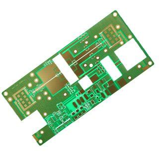
- The corners of the transmission line should be 45° to reduce return loss (Figure 1);
- Use high-performance insulating circuit boards with strictly controlled insulation constant values according to the level. This method is conducive to the effective management of the electromagnetic field between the insulating material and the adjacent wiring.
- Improve the PCB design specifications for high-precision etching. Consider the total error of the line width of +/-0.0007 inches, manage the undercut and cross-section of the wiring shape, and specify the plating conditions of the wiring sidewall. Overall management of the wiring (conductor) geometry and coating surface is very important to solve the skin effect problems related to microwave frequencies and achieve these specifications.
- Prominent leads have tapped inductance and avoid using components with leads. In high-frequency environments, it is best to use surface-mount components.
- For signal vias, avoid using the through-hole processing (PTH) process on sensitive boards because it will cause lead inductance at the via. For example, when a via on a 20-layer board is used to connect layers 1 to 3, the lead inductance can affect layers 4 to 19.
- Provide abundant ground planes. Use molded holes to connect these ground planes to prevent the influence of 3D electromagnetic fields on the circuit board.
- Choose electroless nickel plating or immersion gold plating instead of HASL plating. This electroplated surface can provide better skin effect for high-frequency current (Figure 2). In addition, this highly solderable coating requires fewer leads, which helps reduce environmental pollution.
- The solder mask prevents the flow of solder paste. However, due to the uncertainty of thickness and the unknown insulation performance, covering the entire board surface with solder mask will lead to large changes in electromagnetic energy in microstrip designs. Solder dam is generally used as solder mask.
If you are not familiar with these methods, you can consult experienced design engineers who have worked on military microwave circuit boards
. You can also discuss with them the price range you can afford. For example, using a copper-backed coplanar microstrip design is more economical than a stripline design, and you can discuss this with them to get better advice. Good engineers may not be used to considering cost issues, but their advice is also very helpful. Now we should try to train young engineers who are not familiar with RF effects and lack experience in dealing with RF effects. This will be a long-term task.
In addition, other solutions can be adopted, such as improving computer models to enable them to handle RF effects.
3.PCB and external device interconnection
Now we can think that we have solved all signal management problems on the board and the interconnection of each discrete component. So how to solve the signal input/output problem from the circuit board to the wire connecting the remote device? Trompeter Electronics, an innovator in coaxial cable technology, is committed to solving this problem and has made some important progress (Figure 3). In addition, look at the electromagnetic field given in Figure 4. In this case, we manage the transition between microstrip and coaxial cable. In coaxial cable, the ground layer is annularly interwoven and evenly spaced. In microstrip, the ground plane is below the active line. This introduces certain edge effects that need to be understood, predicted, and accounted for during design. Of course, this mismatch also results in return loss, which must be minimized to avoid noise and signal interference.
Managing impedance issues within the board is not a design issue that can be ignored.
Impedance starts at the surface of the board, then passes through a solder joint to the connector and finally ends at the coaxial cable. Since impedance varies with frequency, the higher the frequency, the more difficult it is to manage impedance. The problem of transmitting signals at higher frequencies over broadband seems to be the main problem faced in design.
Summary
PCB platform technology needs to continue to improve to meet the requirements of integrated circuit designers. The management of high-frequency signals in PCB design and the management of signal input/output on the PCB board need to continue to improve. Whatever exciting innovations will happen in the future, I think bandwidth will continue to increase, and the use of high-frequency signal technology is the prerequisite for achieving this continuous increase in bandwidth
.