Basic Rules and Principles of Switch Mode Power Supply PCB Layout
Introduction
Switch Mode Power Supplies (SMPS) have become ubiquitous in modern electronics due to their high efficiency, compact size, and excellent power handling capabilities. However, the performance of an SMPS design heavily depends on the quality of its printed circuit board (PCB) layout. A poor PCB layout can lead to numerous issues including excessive electromagnetic interference (EMI), thermal problems, unstable operation, and even complete failure of the power supply. This article explores the fundamental rules and principles of SMPS PCB layout that every power supply designer should understand.
Understanding SMPS Operation
Before delving into layout specifics, it’s crucial to understand the basic operation of switch mode power supplies. SMPS circuits rapidly switch power transistors between their fully on and fully off states to regulate voltage. This switching action creates high-frequency current pulses with very fast rise and fall times (often in the range of nanoseconds). These fast transitions, while essential for efficient operation, generate significant high-frequency noise that must be properly managed through careful PCB layout.
The three primary current loops in a typical SMPS are:
- The power loop (input capacitor through switches to output capacitor)
- The gate drive loop (controller to switch gate and back)
- The feedback loop (output voltage sensing to controller)
Each of these loops requires special attention during PCB layout to minimize parasitic inductance and ensure proper operation.
Fundamental PCB Layout Rules for SMPS
1. Minimize High-Frequency Current Loops
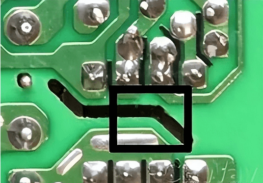
The most critical rule in SMPS PCB layout is to minimize the area of high-frequency current loops. The larger the loop area, the more electromagnetic interference it will radiate. This is particularly important for:
- Input capacitor to switch to output capacitor loop: This loop carries the highest current with the fastest transitions. Keep traces short and wide, and place components close together.
- Gate drive loop: While carrying less current, this loop is sensitive to noise and excessive inductance can slow switching transitions, increasing losses.
2. Proper Grounding Techniques
Grounding in SMPS requires careful consideration:
- Use a star ground for critical reference points to avoid ground loops
- Separate power ground and signal ground, connecting them at a single point
- Use ground planes where possible, but be aware of potential slot antenna effects
- Avoid ground loops which can act as antennas for EMI
3. Component Placement Strategy
Component placement significantly impacts performance:
- Place power components first, arranging them to minimize high-current paths
- Position input capacitors close to switching devices
- Keep control circuitry away from noisy power sections
- Orient components to simplify routing of critical paths
4. Trace Routing Considerations
- Use wide traces for high-current paths to reduce resistance and inductance
- Avoid right-angle bends in high-frequency traces as they increase radiation
- Maintain proper clearance for high-voltage traces
- Route sensitive control signals away from noisy power traces
5. Thermal Management
SMPS components often dissipate significant heat:
- Use adequate copper area for heat dissipation
- Consider thermal relief patterns for easier soldering while maintaining thermal performance
- Place temperature-sensitive components away from heat sources
- Use thermal vias under hot components to transfer heat to other layers
Advanced Layout Principles
1. Parasitic Element Control
Parasitic inductance and capacitance can significantly affect SMPS performance:
- Minimize parasitic inductance in high di/dt paths to reduce voltage spikes
- Control parasitic capacitance in high dv/dt nodes to reduce EMI and losses
- Be aware of inter-layer capacitance in multi-layer boards
2. EMI Reduction Techniques
- Implement proper filtering at input and output
- Use shielding techniques for sensitive circuits
- Consider edge plating to reduce edge radiation
- Optimize switching node layout (the most noisy part of the circuit)
3. Multi-layer Board Strategies
For complex designs using multi-layer PCBs:
- Dedicate entire layers to power or ground where possible
- Use buried layers for sensitive control signals
- Implement proper layer stacking to minimize crosstalk
- Use via stitching to connect ground planes at high frequencies
Practical Implementation Guidelines
1. Input Filter Layout
The input filter is crucial for meeting EMI requirements:
- Place input filter components close to the power entry point
- Maintain good grounding for filter components
- Keep filter traces short and direct
- Avoid routing other traces through the filter area
2. Switching Node Layout
The switching node (connection between switch and inductor) is particularly critical:
- Keep this node as small as physically possible
- Avoid running other traces near the switching node
- Consider using a copper pour for the switching node
- Be mindful of voltage clearance requirements
3. Output Section Layout
The output section requires attention to:
- Proper output capacitor placement near the rectifier
- Adequate trace width for output current
- Proper sensing point for feedback
- Thermal considerations for output components
4. Feedback Network Layout
The feedback network is sensitive to noise:
- Route feedback traces away from noisy areas
- Use guarded traces if necessary
- Keep feedback components close to the controller
- Avoid running feedback traces parallel to power traces
Common Layout Mistakes to Avoid
- Overlooking current return paths: Always consider where currents will flow on their return to source
- Inadequate input capacitor placement: This is one of the most common mistakes
- Poor thermal design: Not providing sufficient copper area for heat dissipation
- Ignoring creepage and clearance requirements: Especially important for high-voltage designs
- Neglecting manufacturability: Designing a layout that cannot be reliably manufactured
Verification and Testing
After completing the PCB layout:
- Perform design rule checks (DRC) for manufacturing requirements
- Run signal integrity simulations if possible
- Prototype and test for proper operation and EMI performance
- Use thermal imaging to identify hot spots
- Perform conducted and radiated EMI testing
Conclusion
Proper PCB layout is essential for achieving optimal performance, reliability, and regulatory compliance in switch mode power supplies. By understanding and applying the fundamental rules and principles outlined in this article—minimizing high-frequency loops, implementing proper grounding, strategic component placement, careful trace routing, and effective thermal management—designers can create SMPS circuits that meet their performance targets while minimizing EMI and thermal issues. Remember that SMPS layout is as much an art as it is a science, and experience combined with careful attention to detail will yield the best results. Always prototype and test your designs thoroughly, as even small layout changes can sometimes have significant impacts on performance.

