Best pcb design
Essential Tips For Optimizing Best pcb design
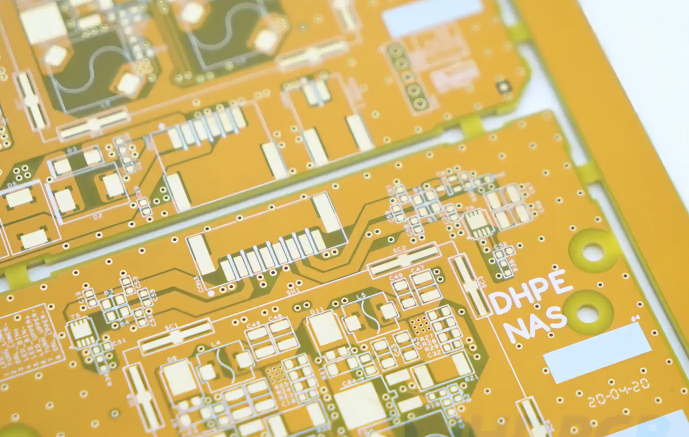
When it comes to optimizing PCB layout, there are several essential tips that can significantly enhance the performance, reliability, and manufacturability of your printed circuit board.
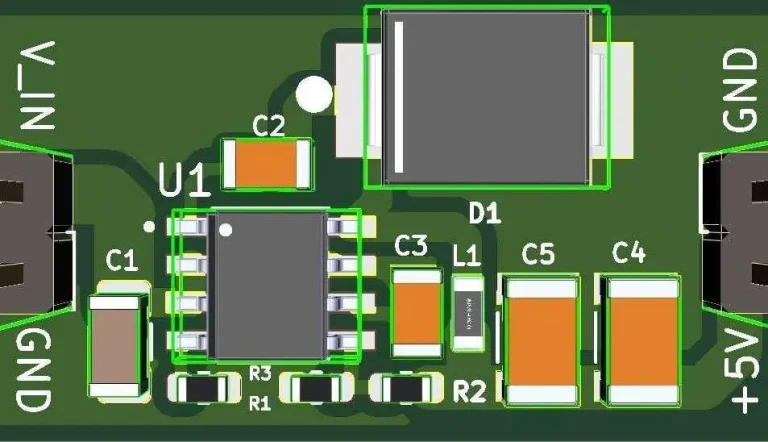
One of the first considerations is component placement. Proper placement is crucial as it directly impacts the ease of routing and the overall functionality of the PCB.
Components should be arranged logically, with related components placed close to each other to minimize trace lengths and reduce potential signal interference. Additionally, placing components in a manner that facilitates heat dissipation can prevent overheating and ensure the longevity of the board.
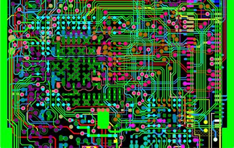
Transitioning to the next critical aspect, trace routing is another fundamental element in PCB design.
Efficient routing not only ensures signal integrity but also minimizes electromagnetic interference (EMI). It is advisable to keep high-speed signal traces as short as possible and to use differential pairs for high-speed data lines to reduce noise. Furthermore, maintaining consistent trace widths and avoiding sharp angles can prevent signal reflection and loss. Utilizing ground planes and power planes effectively can also help in reducing noise and providing a stable reference for signal traces.
Another important consideration is the selection of materials. The choice of substrate material can affect the electrical performance and thermal management of the PCB.
High-frequency applications may require materials with low dielectric constants and low loss tangents to maintain signal integrity. On the other hand, for power electronics, materials with high thermal conductivity are preferred to manage heat dissipation effectively. Therefore, understanding the specific requirements of your application is essential in selecting the appropriate materials.
Moreover, the importance of design for manufacturability (DFM) cannot be overstated.
Ensuring that your PCB design is manufacturable can save time and costs during production. This involves adhering to the design rules and guidelines provided by your PCB manufacturer, such as minimum trace widths, spacing, and hole sizes. Additionally, incorporating test points and considering panelization can facilitate easier testing and assembly, further streamlining the manufacturing process.
In addition to these technical aspects, it is also beneficial to leverage advanced design tools and software.
Modern PCB design software offers a plethora of features that can aid in optimizing your layout. For instance, auto-routing tools can help in efficiently routing complex boards, while simulation tools can predict potential issues such as signal integrity problems and thermal hotspots. Utilizing these tools can significantly enhance the quality and reliability of your PCB design.
Furthermore, collaboration and communication with your team and stakeholders are vital throughout the design process.
Regular reviews and feedback sessions can help identify potential issues early on and ensure that the design meets all requirements and specifications. This collaborative approach can also foster innovation and lead to more effective solutions.
Lastly, thorough testing and validation are indispensable steps in the PCB design process.
Prototyping and testing your design under real-world conditions can uncover issues that may not be apparent during the design phase. This allows for necessary adjustments and refinements before mass production, ensuring that the final product performs as intended.
In conclusion, optimizing PCB layout involves a combination of strategic component placement, efficient trace routing, careful material selection, adherence to manufacturability guidelines, utilization of advanced design tools, effective collaboration, and rigorous testing. By paying attention to these essential tips, you can create a high-performance, reliable, and manufacturable PCB that meets the demands of your application.

Top Software Tools For PCB Design
When it comes to designing printed circuit boards (PCBs), selecting the right software tool is crucial for ensuring efficiency, accuracy, and overall success in your projects. The market offers a plethora of options, each with its unique features and capabilities. To help you navigate this landscape, we will explore some of the top software tools for PCB design, highlighting their strengths and what makes them stand out.
One of the most widely recognized tools in the industry is Altium Designer.
Known for its comprehensive suite of features, Altium Designer offers a seamless integration of schematic capture, PCB layout, and design rule checking. Its user-friendly interface and powerful simulation capabilities make it a favorite among professionals. Additionally, Altium Designer’s extensive library of components and real-time collaboration features facilitate efficient teamwork, making it an excellent choice for both individual designers and larger teams.
Transitioning to another popular option, Eagle by Autodesk is a versatile tool that caters to both beginners and experienced designers.
Eagle’s modular design allows users to customize their workspace according to their needs, providing a balance between simplicity and advanced functionality.
The software’s extensive component library and intuitive routing tools streamline the design process, while its integration with Autodesk’s Fusion 360 enables seamless mechanical and electrical design collaboration. This makes Eagle particularly appealing for projects that require a high level of precision and coordination.
Next, we have KiCad, an open-source PCB design tool that has gained significant traction in recent years.
KiCad’s appeal lies in its cost-effectiveness and robust feature set, which rivals many commercial software packages. The tool offers a comprehensive suite of applications, including schematic capture, PCB layout, and a 3D viewer.
KiCad’s active community of users and developers continuously contribute to its improvement, ensuring that it remains a competitive option for both hobbyists and professionals. Its open-source nature also means that users can customize the software to suit their specific needs, providing a level of flexibility that is hard to match.
Moving on, OrCAD by Cadence is another heavyweight in the PCB design arena.
OrCAD is renowned for its powerful simulation and analysis tools, which are essential for ensuring the reliability and performance of complex designs. The software’s advanced routing capabilities and extensive component libraries make it a go-to choice for high-speed and high-density PCB designs. OrCAD’s integration with other Cadence tools further enhances its appeal, providing a comprehensive solution for electronic design automation (EDA).
Lastly, we must mention DipTrace, a user-friendly PCB design tool that strikes a balance between simplicity and functionality. DipTrace offers an intuitive interface that is easy to navigate, making it an excellent choice for beginners. Despite its simplicity, DipTrace does not compromise on features, offering a range of tools for schematic capture, PCB layout, and 3D modeling. The software’s real-time design rule checking and extensive component library ensure that users can create accurate and reliable designs with ease.
In conclusion, the choice of PCB design software depends on various factors, including the complexity of your projects, your level of expertise, and your specific requirements. Altium Designer, Eagle, KiCad, OrCAD, and DipTrace each offer unique advantages that cater to different needs and preferences. By carefully evaluating these options, you can select the tool that best aligns with your goals, ensuring a smooth and successful PCB design process.
Common Mistakes To Avoid In PCB Design
When embarking on the journey of PCB design, it is crucial to be aware of common pitfalls that can compromise the functionality and reliability of your final product.
One of the most frequent mistakes is neglecting to consider the design for manufacturability (DFM).
This oversight can lead to issues during the production phase, such as difficulties in assembly or increased costs. To avoid this, it is essential to collaborate closely with your manufacturer from the outset, ensuring that your design adheres to their specific capabilities and constraints.
Another prevalent error is inadequate component placement.
Poorly positioned components can result in signal integrity issues, thermal problems, and even mechanical stress. To mitigate these risks, it is advisable to follow best practices for component placement, such as keeping high-speed signals short and direct, placing decoupling capacitors close to power pins, and ensuring adequate spacing between components to facilitate heat dissipation.
In addition to component placement, improper routing of traces can also lead to significant issues.
For instance, failing to maintain consistent trace widths can cause impedance mismatches, which in turn can lead to signal reflections and data corruption. To prevent this, it is important to adhere to the recommended trace width guidelines for your specific application and to use controlled impedance routing where necessary. Furthermore, avoiding sharp angles in trace routing can help minimize signal degradation and electromagnetic interference (EMI).
Grounding is another critical aspect of PCB design that is often overlooked. A poor grounding strategy can result in noise and interference, which can severely impact the performance of your circuit. To ensure a robust grounding scheme, it is advisable to use a solid ground plane, minimize the number of vias, and ensure that all ground connections are as short and direct as possible. Additionally, separating analog and digital grounds can help reduce noise coupling between different sections of your circuit.
Thermal management is another area where designers frequently make mistakes.
Failing to account for heat dissipation can lead to overheating, which can damage components and reduce the overall lifespan of your PCB. To address this, it is important to consider the thermal properties of your materials, use thermal vias to transfer heat away from critical components, and incorporate heat sinks or other cooling mechanisms as needed.
Moreover, overlooking the importance of design rule checks (DRCs) can result in a myriad of issues. DRCs are essential for ensuring that your design adheres to the manufacturing constraints and industry standards. By regularly running DRCs throughout the design process, you can catch potential errors early and avoid costly revisions later on.
Lastly, insufficient documentation can create challenges during the manufacturing and assembly stages.
Providing comprehensive documentation, including detailed schematics, bill of materials (BOM), and assembly drawings, is crucial for ensuring that your design is accurately and efficiently produced. Clear and thorough documentation can also facilitate troubleshooting and maintenance down the line.
In conclusion, avoiding these common mistakes in PCB design requires a combination of careful planning, adherence to best practices, and close collaboration with your manufacturing partners. By being mindful of design for manufacturability, component placement, trace routing, grounding, thermal management, design rule checks, and documentation, you can significantly enhance the reliability and performance of your PCB, ultimately leading to a more successful and cost-effective product.

Advanced Techniques For High-Speed PCB Design
Designing high-speed printed circuit boards (PCBs) requires a meticulous approach, as the performance of these boards is critical in modern electronic devices.
To achieve optimal functionality, engineers must employ advanced techniques that address the unique challenges posed by high-speed signals.
One of the primary considerations in high-speed PCB design is signal integrity,
which can be compromised by factors such as crosstalk, electromagnetic interference (EMI), and signal reflection. To mitigate these issues, designers must carefully plan the layout and routing of the PCB.
Firstly, the use of controlled impedance traces is essential.
Controlled impedance ensures that the signal travels through the PCB without significant distortion, which is crucial for maintaining signal integrity. This involves calculating the trace width and spacing based on the dielectric properties of the PCB material and the desired impedance. Additionally, differential signaling can be employed to further enhance signal integrity. Differential pairs, which consist of two traces carrying equal and opposite signals, are less susceptible to noise and crosstalk, making them ideal for high-speed applications.
Another critical aspect of high-speed PCB design is the management of power distribution.
Proper power distribution is vital to ensure that all components receive a stable and clean power supply. This can be achieved through the use of power planes, which provide a low-impedance path for the current and help to reduce noise. Decoupling capacitors should be strategically placed near power pins to filter out high-frequency noise and provide a stable voltage supply to the components.
Thermal management is also a significant concern in high-speed PCB design.
High-speed circuits tend to generate more heat, which can affect the performance and reliability of the PCB. To address this, designers can use thermal vias and heat sinks to dissipate heat away from critical components. Additionally, the placement of components should be optimized to ensure adequate airflow and prevent hotspots.
The choice of materials plays a crucial role in high-speed PCB design.
High-frequency signals require materials with low dielectric constant and low loss tangent to minimize signal attenuation and distortion. Common materials used in high-speed PCBs include FR-4, Rogers, and Teflon. Each material has its own set of properties, and the selection should be based on the specific requirements of the application.
Furthermore, the use of simulation tools is indispensable in high-speed PCB design.
Simulation allows designers to model the behavior of the PCB and identify potential issues before the board is fabricated. Tools such as signal integrity simulators and electromagnetic field solvers can provide valuable insights into the performance of the PCB and help to optimize the design.
In addition to these techniques, adhering to design guidelines and best practices is essential for successful high-speed PCB design.
This includes maintaining consistent trace widths, minimizing the length of high-speed traces, and avoiding sharp corners in the routing. Proper grounding is also crucial, as a solid ground plane can help to reduce EMI and improve signal integrity.
In conclusion, high-speed PCB design is a complex and challenging task that requires a thorough understanding of various factors that can affect signal integrity and overall performance.
By employing advanced techniques such as controlled impedance, differential signaling, proper power distribution, thermal management, and the use of simulation tools, designers can create high-speed PCBs that meet the demanding requirements of modern electronic devices. Adhering to best practices and carefully selecting materials further ensures the reliability and efficiency of the final product.