Best PCB Layout Tips for Gate Driver ICs
Infineon’s 1ED44173/5/6 are new low-side gate driver ICs that integrate overcurrent protection (OCP), fault status output, and enable functions. This highly integrated driver is very friendly for PFC (digitally controlled power factor correction) applications using boost topology and ground reference.
In PFC applications, shunts are used to sample the power switch current or DC bus current. The location of the shunt varies depending on the selected control method. For example, in Figure 1 Example 1, the shunt is located between the IGBT emitter and system ground to sample the power switch current when the controller implements peak current control or current balance control in interleaved PFC applications.
In contrast, Figure 1 Example 2 shows a shunt located between system ground and the negative pole of the DC bus to sense the DC bus current. This configuration is often used in average current mode control, where the digital controller can calculate the input power based on the average current and DC bus voltage feedback.
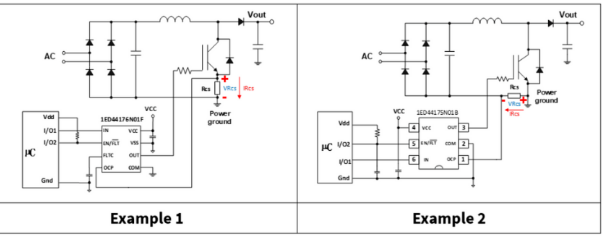
Figure 1: Two different types of low-side gate drivers with OCP: 1ED44176N01F (Example 1) with positive current sensing to meet the requirements of the first shunt position, while 1ED44173/5N01B (Example 2) with negative current sensing to meet the requirements of the second shunt position
Applications in residential air conditioners
In today’s residential air conditioning (RAC) applications with digitally controlled PFC, the controller uses the power feedback signal to implement adaptive DC bus voltage control. This allows for reduced losses at light loads when a lower DC bus voltage is used, while switching to the full DC bus when full load is required.
Due to different shunt configurations, Infineon designed two different types of low-side gate drivers with OCP: 1ED44176N01F (Figure 1, Example 1), and 1ED44173N01B and 1ED44175N01B (Figure 1, Example 2). The former has positive current sensing to meet the shunt configuration of Example 1, while the latter two have negative current sensing to meet the shunt configuration of Example 2. The 1ED44175N01B is targeted at driving IGBTs, while the 1ED44173N01B is targeted at driving MOSFETs.
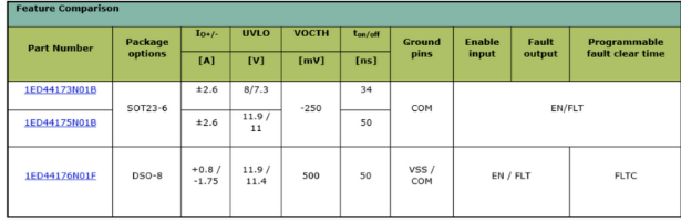
Figure 2: Differences in 1ED44173/5/6 functions
PCB layout is always a challenge in high-current, high-speed switching circuits such as PFC. A good PCB layout can ensure device operating conditions and design stability. Improper components or layout may cause switching instability, excessive voltage ringing, or circuit latch-up.
Best PCB layout tips for gate driver ICs
- When using RC filtering circuits between the microcontroller and the gate driver, keep the input wiring as short as possible (less than 2-3 cm).
- The EN/FLT output is an open-drain output, so a pull-up resistor is required to pull it to the 5V or 3.3V logic power supply. When designing, place the RC filter close to the gate driver.
- To prevent false triggering in overcurrent protection, the RC filter wiring between OCP and ground should be as short as possible.
- Install each capacitor as close to the gate driver pin as possible.
- Connect the microcontroller ground line directly to the COM pin (1ED44173/5N01B).
- Connect the gate output return to COM and the microcontroller ground pin to the VSS logic ground pin (1ED44176N01F), which can prevent noise coupling from the logic input pin to the driver output return.
Let’s see what a proper layout can do. The following example shows the circuit (Figure 3) and layout implementation (Figure 4) of 1ED44175N01B and TO-247 IGBT (e.g. IKW40N65WR5). With this design, the loop area and inductance of the PCB can be reduced.
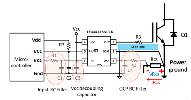
Figure 3: Circuit diagram of 1ED44175N01B
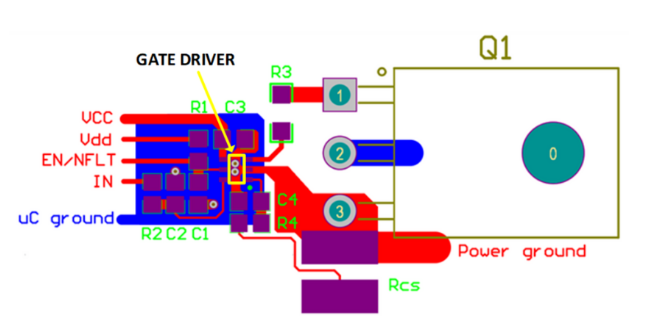
Figure 4: PCB layout of the above circuit
How to reduce the PCB trace encirclement area to reduce parasitic inductance
● Place 1ED44175N01B close to the gate and emitter of the IGBT
● Place the decoupling capacitor (C3) directly on the VCC and COM pins
● Place the filter capacitors (C1 and C4) and the fault clearing time programming capacitor (C2) close to the pins
● Place the ground plane just above or just below the 1ED44175N01B to reduce the trace inductance
In addition, the ground plane connected to COM helps as a shield for radiated noise and provides a heat dissipation path for the device to dissipate power. Following these layout tips can eliminate common noise coupling problems and save you development time.
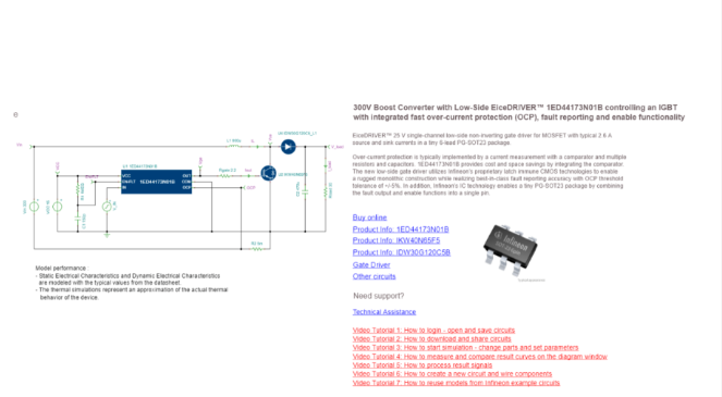
Figure 5: Online simulation page


