Beyond recycling,PCBs themselves are also going green
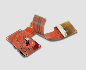
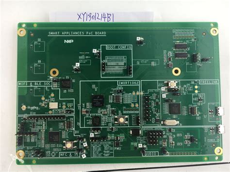
In the lab of JIAN Technology,an engineer Picked up a shiny flexible printed circuit board(FPC)about to be processd in a new low-carbon manufacturing facility.This wasn’t just any ordinary PCB;it epitomized the electronics industry’s green transformation.
At an industry exchange conference in Taipei,JIAN Technology,the Industrial Technology Reserach institute(ITRI),and the Institute for information Industry(IITI)jointly signed a cooperation agreement in March 2025 to form the”Low-Carbon,Energy-saving FPC 2.0 joint R&D Alliance.”
The event lacked dazzling lights and stage presence,but it attracted numerous companies from across the supply chain,Their focus was clear: how to make printed circuit boards(PCBs),the lifeblood of the electronics industry,more environmentally friendly.
At the same time,Lite-On Technology announced a deepening partnership with Japanese startup Elephantech to promote investment in and application of low-carbon printed circuit board technology,introducing it to existing partner factories and upgrading production lines.

1.Why focus on the”green revolution”of PCBs?
Electronic waste has become one of the fastest-growing waste streams globally,and printed circuit boardz(PCBs),the backbone of nearly all electronic devices,play a crucial role.
According to industry statistics,millions of tons of PCB waste are generated globally each year,and the amount continues to grow at an annual rate of 5%-8%.
If improperly handled,these discarded PCBs not only occupy significant land resources but also cause serve pollution to soil,water,and air due to the presence of heavy metals such as lead,mercury,and cadmium,as well as hazardous substances such as brominated flame retardants.
Traditional PCB manufacturing processes also face significant environmental challenges. According to a report by IDTechEx, energy and water usage in the semiconductor industry will increase at a compound annual growth rate of 12% and 8%, respectively, from 2025 to 2035.
Faced with such a dire situation,improving recycling technology alone is clearly insufficient.A green PCB transformation,starting from the source,is urgently needed.
2.Three Paths to Greening PCBs
The green transformations of PCBs is unfolding comprehensive across three key areas:materials,design,and manufacturing technology,Each advancement marks a soild step forward for the industry towards sustainable development.
New Materials:Breakthroughs in Bio-based and Degradable material
The industry is exploring alternatives to traditional PCB substrates with bio-based polymer or low-toxicity resins.
These emerging materials include polylactic acid, Soluboard®, Recyclad1G, and ReUSE®, which are expected to replace the currently dominant FR4 material in the long term.
Japanese startup Elephantech has developed low-carbon printed circuit board technology,which reduces water and copper consumption during production through innovative applications.
Liteon Technologies has invested in Elephanctech’s manufacturing equipment and introduced it to partner factories,demonstrating the trend of traditional electronics components embracing green manufacturing.
New Design:The Emergence of Design for Recycling
The 2025 revision of the EU WEEE Directive requires that circuit board designs adhere to Design for Recyclability(DfR)principles.
Modular design is key,allowing for disassembly and recycling rather than complete scrapping.
Designing for easy-to-disassemble connections,such as removeable connectors instead of solderd components,reduces recycling complexity.
These design changes not only improve PCB recyclability but also reduce the amount of electronic waste generated at the source,
New Technology: Low-Carbon Manufacturing Processes
The PCB manufacturing industry is exploring low-temperature processing to optimize or eliminate unnecessary and wasteful process steps and maximize material recovery and reuse.
Emerging technologies such as inkjet SAP are demonstrating potential for low-carbon and material-saving applications.
The “Low-Carbon and Energy-Saving Flexible PCB 2.0” alliance, a collaboration between Jialianyi Technology and research institutions, is collaborating in depth on areas such as automated equipment and transparent substrate applications to improve overall technology density and process yield.
03 Technical Bottlenecks of Green PCBs
While green PCB technology holds great promise, its development faces numerous challenges that hinder its large-scale commercial application.
Material performance is a primary consideration. Currently, most environmentally friendly substrate materials struggle to fully replace traditional materials in terms of thermal conductivity, mechanical strength, and durability.
As electronic products evolve toward higher frequencies and higher speeds, the performance of green PCB materials in high-frequency signal transmission remains to be verified.
Cost is also a significant issue. Emerging green PCB manufacturing technologies often require expensive specialized equipment and processes, which can be a significant burden for small and medium-sized enterprises with limited profit margins.
A Belgian smelter’s proposed waste PCB metal recycling program, while offering significant environmental benefits, comes with high initial equipment investment costs.
Technology integration is also a major challenge. Integrating new green materials or processes into existing PCB manufacturing processes is highly complex.
The global electronics supply chain is vast and complex, and any fundamental change requires collaborative efforts from upstream and downstream of the supply chain.
04 Driving the Green PCB Industry with Both Regulations and Markets
Increasingly stringent environmental regulations and maturing market mechanisms worldwide are accelerating the green transformation of PCBs.
Increasingly Stringent Regulations
The EU’s Waste Electrical and Electronic Equipment (WEEE) Directive was revised in 2025, requiring a minimum recycling rate of 85% for circuit boards, with at least 50% of the materials being reused or recycled.
The WEEE Directive also strengthens the Extended Producer Responsibility (EPR) system, requiring manufacturers to prepay e-waste disposal costs when their products are put on the market.
In February 2025, China’s Ministry of Ecology and Environment and the Ministry of Finance jointly issued the “Notice on the Standards and Conditions for Enterprises Applying for Special Funds for the Treatment of Waste Electrical and Electronic Products,” guiding enterprises to improve resource and environmental benefits through financial incentives.
Broad Market Opportunities
Growing consumer awareness of environmental protection is making green electronic products more attractive in the market.
By adopting green PCB technology, companies can not only meet regulatory requirements but also reduce long-term costs and enhance their brand image.
For technologically advanced companies, green PCB technology presents a market opportunity to differentiate their products and gain a competitive advantage.
05 The Road Ahead: Where is Green PCB Headed?
Looking ahead, the green development of PCBs will demonstrate a diversified, technology-driven, and globally collaborative trend, all of which will collectively shape the future of sustainable development for the electronics industry.
Technological innovation will continue to advance. An IDTechEx report predicts that from 2025 to 2035, additive manufacturing is expected to reduce costs and minimize waste in the PCB industry.
Innovative metal recovery technologies such as biometallurgy have also shown potential, leveraging the metabolic activity of microorganisms to achieve low-energy, high-purity metal extraction.
Policy coordination will become increasingly important. The EU’s Digital Product Passport (DPP) regulation, which will take effect in 2025, will provide greater transparency into the flow of e-waste.
Although 90% of printed circuit boards are manufactured in the Asia-Pacific region, the electronics supply chain is global, so regulations in various regions have broad global implications.
Industry chain collaboration will become mainstream. For example, Jialianyi Technology has partnered with the Industrial Technology Research Institute, the Institute for Information Industry, and several upstream and downstream companies to form a research and development alliance to integrate resources and achieve collaborative development.
Lite-On Technology is integrating green manufacturing into product development through collaboration with startups, exemplifying collaborative innovation across the supply chain.
Globally, millions of tons of PCB waste are generated annually, and the waste continues to grow at a rate of 5%-8% annually. In Taiwan, Japan, Europe, and the United States, a growing number of companies are integrating sustainability into every aspect of the PCB lifecycle.
From biodegradable substrates to low-carbon manufacturing processes, from modular designs to closed-loop recycling systems, the green transformation of PCBs is resonating throughout the electronics industry chain.
“The era of siloed efforts is over,” Jialianyi Technology emphasized at an industry exchange meeting. “Building a systematic R&D collaboration platform is the key to driving flexible PCB manufacturing towards high-value, low-carbon manufacturing.”