BGA package design and common defects
Correctly Design the BGA Package
Ball Grid Array (BGA) is becoming a standard packaging form. People have seen significant results using BGAs with a pitch of 0.05 to 0.06 inches. The next step in packaging evolution is likely to be chip-scale packaging (CSP), which is smaller and easier to process.
BGA design rules
Bump slump technology, where the endpoints of tin and lead balls sink to the substrate to form solder joints during reflow soldering, can be traced back to the mid-1970s. But only now is it starting to develop rapidly. Currently, companies such as Motorola, IBM, Citizen, ASAT, LSI Logic, Hestia and Amkor, in addition to using this package in their own products, also provide BGA products.
Another major advantage of BGA is its high yield. Users such as Motorola and Compaq claim no defects in their 0.05-inch pitch packages containing 160 to 225 I/O leads. In other fully automated factories, the failure rate of fine-pitch devices with the same I/O lead count is 500 or 1000PPM. BGA packages with 400 to 700 I/O leads are currently being further developed, and Japan has even reported the development results of BGA packages with 1,000 I/O leads. At present, the standard has not been fully formulated, and the JEDEC document only provides basic provisions for 1mm, 1.27mm and 1.5mm spacing. The size of the substrate ranges from 7 to 50 mm, and the coplanarity is less than 200 μm.

Limitations of BGA
Many users complain about poor visibility of BGA solder joints. Obviously, the solder joints of BGA cannot be inspected with the naked eye. In fact, this is the case with any modern electronics assembly process due to ever-increasing component lead counts. Relatively simple inspections can be performed using low-cost X-ray equipment and good design rules.
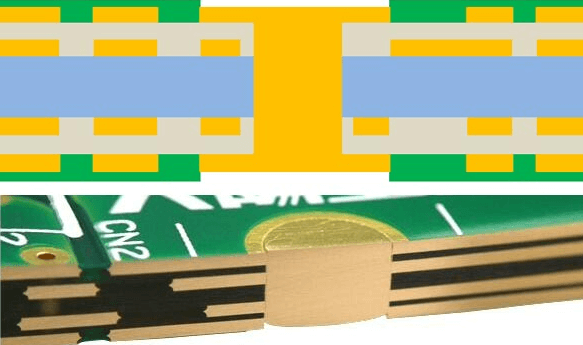
Today’s routing footprint includes printed wire assemblies, through holes, and 0.02-inch circular surface pads. The size of the solder balls on the device will inevitably affect the pad size. Initially, some engineers applied solder mask to the pad surface to reduce device movement and solder paste flow during reflow. With this method, the solder joints are prone to cracking during the heating process, so it is not advisable.
If there is a standard gap between the copper pad and the solder mask coating, then standard solder mask design rules should be used. This simple layout allows traces to be routed on both surfaces of the PCB if needed. Even devices with a pitch of 1 or 1.27mm and a large number of I/Os will have wiring problems between the solder balls. This problem can be overcome by choosing a device with a small pitch but a “blank” center (i.e. no solder ball). The outer edge of the BGA with a blank center may have only four rows of solder balls, reducing routing problems.
Through hole mounting
Some companies use traditional through holes as mounting pads for ceramic BGAs and more commonly used plastic devices. At this point, the vias become the mounting pads and interconnects through the printed board. This is ideal for reflow soldering designs, but not for wave soldering products. Remember: Wave soldering operations will cause secondary reflow of the BGA on the top of the printed board.
When using the through-hole mounting method, ensure that the volume of the through hole matches the amount of solder paste printed. With this technique, the solder paste will fill the via and still provide the same standoff after reflow. If this important factor is not taken into consideration, the solder ball portion will sink into the solder joint. For ceramic BGAs, high-temperature solder balls can only be located on the surface of the via. When the via size is reduced, the problem becomes less severe. But when routing internally, it does affect the routing of complex multi-layer printed boards.
The underfill of the printed board can be tested through the top of the via connected to the selected test pad. In some cases, component manufacturers set test points on the top of the BGA package substrate to directly probe the package surface. If through-hole mounting is used in assembly operations, testing can be performed by directly probing the through-holes.
Beware of warping
Larger plastic packages may warp during reflow soldering. In some cases, warpage of the over-molding compound and substrate is seen, which results in minimal contact of the external connection points to the pads. Some engineers point out that both die and glass-epoxy substrates can warp. This problem can be overcome to some extent by improving the layout of the spherical endpoints of the parts and limiting the size of the die used. If a solder paste is used instead of just a flux reflow process, the likelihood of this particular failure is reduced because the solder paste has lower coplanarity requirements.
For traditional glass/epoxy resin substrates, using leadless plastic BGA will prevent welding failures. Because the part base is also made from a similar epoxy resin, the coefficient of thermal expansion matches that of most applications. In some specialized applications, cracks may develop in the solder joints at the corners of the device, possibly due to stress generated there.
For plastic BGA devices, “popcorn” cracks may appear. Because during reflow soldering, moisture will expand inside the component. At this point, cracks will appear at the edge of the device between the substrate and cladding. If this phenomenon occurs during rework, you will hear the device making a popping sound, hence the name “popcorn.” Therefore, appropriate moisture-proof packaging must be selected to reduce the possibility of bursting