Blister PCB Assembly: A Comprehensive Guide
Introduction
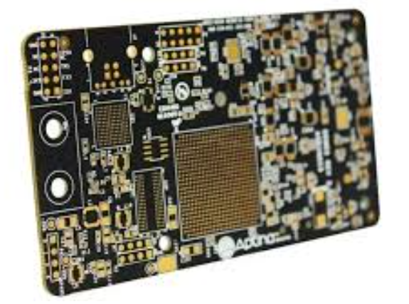
Printed Circuit Board (PCB) assembly is a critical process in electronics manufacturing, involving the placement and soldering of components onto a PCB to create functional electronic devices. Among various assembly techniques, blister PCB assembly is a specialized method used for specific applications where reliability, protection, and compactness are essential.
This article explores blister PCB assembly in detail, covering its definition, advantages, manufacturing process, applications, and key considerations for successful implementation.
What is Blister PCB Assembly?
Blister PCB assembly refers to a packaging and assembly technique where a PCB is enclosed in a protective “blister” or molded casing, typically made of plastic or another insulating material. This method is commonly used in applications where the PCB needs to be shielded from environmental factors such as moisture, dust, chemicals, or mechanical stress.
The term “blister” comes from the resemblance of the casing to a blister pack, where the PCB is securely embedded within a cavity, leaving only necessary connectors or interfaces exposed.
Advantages of Blister PCB Assembly
Blister PCB assembly offers several benefits, making it suitable for demanding applications:
1. Enhanced Protection
- Shields PCBs from moisture, dust, and corrosive environments.
- Provides mechanical protection against vibrations and impacts.
2. Improved Reliability
- Reduces the risk of short circuits and electrical interference.
- Extends the lifespan of electronic components.
3. Compact and Lightweight Design
- Allows for space-efficient PCB integration in small devices.
- Ideal for wearable electronics, medical devices, and automotive applications.
4. Customizable Enclosures
- The blister casing can be tailored to fit specific PCB shapes and sizes.
- Can include features such as heat dissipation channels or EMI shielding.
5. Cost-Effective for High-Volume Production
- Injection-molded blister casings are economical for mass production.
- Reduces the need for additional protective coatings or conformal coatings.
The Blister PCB Assembly Process
The assembly of a blister-encased PCB involves several key steps:
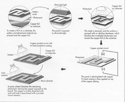
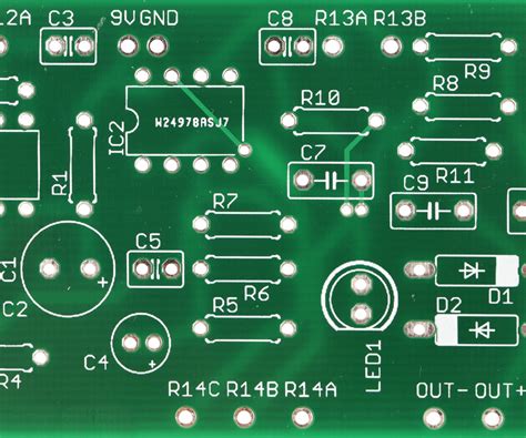
1. PCB Design and Fabrication
- The PCB is designed with consideration for the blister casing dimensions.
- Components are placed to avoid interference with the enclosure.
2. Component Placement and Soldering
- Surface Mount Technology (SMT) or Through-Hole Technology (THT) is used to assemble components.
- Automated pick-and-place machines ensure precision.
3. Testing and Inspection
- The assembled PCB undergoes electrical testing (e.g., in-circuit testing, functional testing).
- Automated Optical Inspection (AOI) checks for soldering defects.
4. Encapsulation in the Blister Casing
- The PCB is placed into a pre-molded plastic blister.
- The casing is sealed using ultrasonic welding, adhesive, or heat staking.
5. Final Quality Assurance
- The encapsulated PCB is tested for environmental resistance (e.g., IP rating validation).
- Mechanical stress tests ensure durability.
Applications of Blister PCB Assembly
Blister PCB assembly is widely used in industries requiring robust and compact electronics:
1. Medical Devices
- Implantable and wearable medical sensors.
- Diagnostic equipment requiring sterilization resistance.
2. Automotive Electronics
- Engine control units (ECUs) exposed to harsh conditions.
- LED lighting modules with waterproof requirements.
3. Consumer Electronics
- Water-resistant smartwatches and fitness trackers.
- Durable IoT devices for outdoor use.
4. Industrial Automation
- Sensors and control modules in manufacturing environments.
- Robotics with vibration-resistant electronics.
5. Aerospace and Defense
- Avionics systems requiring shock and moisture resistance.
- Military-grade communication devices.
Key Considerations for Blister PCB Assembly
To ensure a successful blister PCB assembly process, manufacturers must consider the following factors:
1. Material Selection
- The blister casing material should match environmental requirements (e.g., polycarbonate for impact resistance, PPS for high-temperature stability).
2. Thermal Management
- Proper heat dissipation must be ensured to prevent overheating.
- Thermal vias or heat sinks may be integrated into the design.
3. Connector and Interface Accessibility
- Critical ports (USB, power inputs) must remain accessible after encapsulation.
4. Manufacturing Tolerances
- Tight tolerances are required to ensure a snug fit without stressing the PCB.
5. Compliance with Industry Standards
- IPC standards for PCB assembly.
- IEC or MIL-STD certifications for specific applications.
Challenges in Blister PCB Assembly
Despite its advantages, blister PCB assembly presents some challenges:
- Higher Initial Tooling Costs – Custom blister molds can be expensive for low-volume production.
- Design Complexity – PCB layout must account for the blister’s dimensional constraints.
- Repair Difficulties – Once encapsulated, repairing the PCB may require casing destruction.
Future Trends in Blister PCB Assembly
Advancements in materials and manufacturing techniques are shaping the future of blister PCB assembly:
- 3D-Printed Blister Casings – Enabling rapid prototyping and customization.
- Smart Encapsulation Materials – Self-healing polymers for enhanced durability.
- Miniaturization – Thinner, lighter casings for next-gen wearable electronics.
Conclusion
Blister PCB assembly is a highly effective method for protecting electronic circuits in demanding environments. Its advantages in durability, compactness, and reliability make it indispensable in medical, automotive, industrial, and consumer electronics applications. By carefully considering design, material selection, and manufacturing processes, engineers can leverage blister PCB assembly to produce robust and long-lasting electronic devices.
As technology evolves, innovations in encapsulation materials and smart manufacturing will further enhance the capabilities of blister PCB assembly, making it an even more vital technique in electronics production