Board PCBA Evolution: Key Strategies for Advanced Circuit Integration
Key Takeaways
Modern PCB assembly processes have reached unprecedented levels of precision, driven by innovations in PCBA design and manufacturing. Central to these advancements are breakthroughs in circuit density optimization, enabling the integration of complex functionalities within shrinking form factors. Engineers now prioritize thermal management strategies, such as advanced heat dissipation materials and layered cooling architectures, to maintain reliability in high-density layouts.
Equally vital are advancements in signal integrity preservation, achieved through impedance-controlled routing and minimized electromagnetic interference (EMI) in PCBA stacks. These techniques are critical for supporting high-speed data transmission in IoT/AI systems, where latency and noise reduction directly impact performance. Additionally, the adoption of AI-driven manufacturing tools has streamlined prototyping cycles, allowing for real-time adjustments in PCB assembly workflows.
Emerging materials, including low-loss substrates and high-temperature resins, further enhance reliability scaling for mission-critical applications. Together, these strategies form a cohesive framework for next-generation electronics, balancing miniaturization demands with robust operational requirements. As industries push toward smarter, faster devices, the evolution of PCBA technologies remains foundational to achieving seamless circuit integration across sectors.
Board PCBA Circuit Integration Breakthroughs
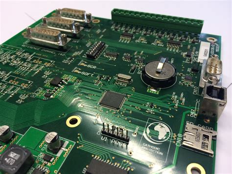
Recent advancements in PCB assembly techniques have redefined the limits of circuit integration, enabling PCBA designs to achieve unprecedented component density while maintaining operational stability. By leveraging high-density interconnect (HDI) architectures and embedded component technology, engineers now integrate passive components directly into substrate layers, reducing surface footprint by up to 40%. This approach not only optimizes space but also minimizes parasitic effects, a critical factor for high-speed circuit performance in AI-driven applications.
Design Tip: When implementing embedded components, prioritize material compatibility to avoid thermal expansion mismatches during PCBA reflow processes.
Modern PCBA workflows increasingly adopt laser-drilled microvias and sequential lamination to support multilayer stacking, achieving signal path lengths under 100µm. These innovations are complemented by advanced substrates like low-loss dielectrics, which reduce crosstalk in high-frequency IoT systems. For instance, 5G-enabled devices now utilize PCB assembly methods that embed antennas within the board structure, eliminating external modules without compromising signal integrity.
"The shift toward 3D-printed conductive traces is unlocking new possibilities for heterogeneous integration in PCBA, particularly for wearable medical devices."
However, achieving reliable circuit integration demands rigorous testing protocols. Automated optical inspection (AOI) systems now incorporate machine learning algorithms to detect micron-level defects in real time, ensuring yield rates above 99.2% even for complex designs. As IoT and AI systems demand tighter integration, PCBA developers must balance component density with thermal and mechanical constraints—a challenge addressed through collaborative design tools that simulate electrical, thermal, and stress behaviors simultaneously.
Smart Thermal Solutions for High-Density PCBA
As PCB assembly designs push toward higher component density to meet demands for compact IoT and AI systems, managing heat dissipation becomes critical. Modern PCBA architectures integrate advanced thermal interface materials (TIMs) like graphene-based pads and phase-change compounds, which improve heat transfer between components and substrates. Engineers now combine embedded copper-core substrates with microfluidic cooling channels to address localized hotspots in high-power circuits. For ultra-dense layouts, laser-drilled thermal vias and active cooling systems using piezoelectric fans ensure stable operation even under sustained workloads.
Transitioning to multi-layer PCBA designs further complicates thermal dynamics, necessitating AI-driven simulation tools to model heat distribution across stacked circuits. Innovations such as thermally conductive adhesives and low-CTE (coefficient of thermal expansion) substrates minimize mechanical stress during thermal cycling, enhancing long-term reliability. These strategies not only optimize PCB assembly performance but also align with the broader shift toward energy-efficient electronics. By balancing material science with precision engineering, manufacturers achieve thermal stability without compromising signal integrity—a cornerstone for next-generation AI-driven devices.
Signal Integrity Optimization in Advanced PCBA
Maintaining signal integrity remains a critical challenge in modern PCB assembly, particularly as PCBA designs push toward higher frequencies and miniaturization. With IoT and AI systems demanding faster data transmission, engineers employ advanced techniques to mitigate signal degradation caused by impedance mismatches, crosstalk, and electromagnetic interference (EMI).
A primary strategy involves optimizing trace geometry through precise impedance matching, ensuring consistent signal propagation across high-speed channels. For instance, differential pair routing reduces noise susceptibility in multi-layer PCBA stacks. Material selection also plays a pivotal role: low-loss dielectric substrates like Rogers 4350B minimize attenuation at frequencies exceeding 10 GHz.
| Technique | Impact on Signal Integrity | Implementation Complexity |
|---|---|---|
| Impedance Matching | Reduces reflections | Moderate |
| EMI Shielding | Lowers interference | High |
| Differential Pairing | Minimizes cross-talk | Low to Moderate |
| Advanced Dielectrics | Enhances high-frequency performance | High |
Additionally, ground plane optimization and via stitching techniques improve return current paths, while 3D electromagnetic simulation tools enable pre-production validation of signal behavior. As PCBA densities increase, integrating embedded passive components further shortens signal paths, reducing latency in AI accelerator modules. These innovations collectively address the growing need for reliable high-speed interconnects in next-generation electronics.
IoT/AI System Enhancements via PCBA Innovations
The rapid proliferation of IoT and AI technologies demands PCBA designs that balance miniaturization with heightened computational capabilities. Modern pcb assembly processes now integrate embedded components and flexible substrates, enabling compact layouts without compromising performance. For instance, system-in-package (SiP) architectures in pcba designs allow seamless integration of sensors, processors, and wireless modules—critical for edge-computing devices requiring low latency and high energy efficiency.
Thermal management remains pivotal, as densely packed circuits in AI accelerators generate significant heat. Advanced pcb assembly techniques employ thermally conductive adhesives and copper-filled vias to dissipate heat efficiently, ensuring stable operation in IoT nodes deployed in harsh environments. Additionally, high-density interconnect (HDI) layers in pcba stacks optimize signal routing, reducing electromagnetic interference (EMI) that could disrupt sensitive AI algorithms.
Another breakthrough lies in adaptive power distribution networks, which dynamically adjust voltage levels to match AI workloads. This innovation, combined with impedance-controlled traces in pcb assembly, enhances signal integrity for high-frequency data transmission—a necessity for real-time analytics in smart factories or autonomous systems. By leveraging these advancements, engineers can scale pcba reliability while meeting the evolving demands of AI-driven IoT ecosystems.
Next-Gen Electronics Miniaturization Strategies
The relentless push toward miniaturization in modern electronics demands innovative approaches to PCB assembly (PCBA) that balance component density with functional reliability. Cutting-edge high-density interconnect (HDI) technologies now enable PCBA designs to accommodate up to 20% more components per square centimeter compared to traditional layouts, driven by advancements in laser-drilled microvias and ultra-fine-pitch soldering. By integrating embedded passive components and leveraging system-in-package (SiP) architectures, engineers reduce spatial footprints while maintaining signal coherence across densely packed circuits.
Thermal management remains critical as component spacing shrinks. Advanced PCBA strategies employ thermally conductive adhesives and embedded heat spreaders to dissipate heat from high-power ICs, ensuring stable operation in compact IoT devices and AI accelerators. Simultaneously, flex-rigid PCB assemblies are gaining traction, allowing three-dimensional configurations that optimize space in wearables and medical implants.
To sustain signal integrity, designers adopt impedance-controlled routing and shielding techniques tailored for millimeter-scale traces. These methods, combined with AI-driven simulation tools, predict electromagnetic interference (EMI) risks early in the PCB assembly process. As industries transition to 5G and edge computing, these miniaturization strategies ensure PCBA platforms meet evolving demands for speed, efficiency, and scalability without compromising durability.
PCBA Material Advances for Reliability Scaling
Recent innovations in PCB assembly materials are addressing critical challenges in reliability for high-performance systems. The shift toward nanocomposite substrates and low-loss dielectrics enables PCBA designs to withstand higher operating temperatures while minimizing signal degradation. Advanced laminates with ceramic fillers, for instance, reduce the coefficient of thermal expansion (CTE) mismatch between components and boards, a persistent issue in multilayer PCB assembly.
Engineers now prioritize halogen-free flame retardants and high-Tg (glass transition temperature) polymers to meet stringent environmental regulations and enhance thermal resilience. These materials not only improve PCBA longevity in harsh environments but also support finer trace geometries required for IoT/AI applications. Additionally, novel conductive adhesives with silver-coated copper particles are replacing traditional solders, offering superior electrical conductivity and resistance to electromigration.
A key breakthrough lies in embedded passives and thermal interface materials (TIMs), which optimize space utilization and heat dissipation in compact designs. For example, graphene-enhanced TIMs achieve 30% better thermal conductivity than conventional options, critical for maintaining signal integrity in densely packed circuits. By integrating these material advancements, manufacturers achieve reliability scaling without compromising on circuit density or performance—a cornerstone for next-generation electronics.
AI-Driven Manufacturing Techniques for PCBA
Modern PCB assembly processes are undergoing radical transformation through artificial intelligence, enabling unprecedented precision in PCBA manufacturing. By integrating machine learning algorithms with automated optical inspection (AOI) systems, manufacturers can now detect microscopic defects—such as solder bridging or misaligned components—with over 99.7% accuracy. These AI-powered systems analyze terabytes of historical production data to predict failure patterns, dynamically adjusting parameters like reflow oven temperatures or stencil pressure in real time.
A key innovation lies in adaptive process optimization, where neural networks continuously refine PCB assembly workflows based on live sensor feedback. For instance, AI-driven pick-and-place machines optimize nozzle selection and placement sequences to handle ultra-fine-pitch components, critical for high-density IoT devices. Additionally, generative AI models simulate PCBA thermal behaviors under varying loads, enabling proactive thermal management strategies that prevent overheating in compact designs.
The shift toward AI also enhances scalability. Cloud-based platforms aggregate data from global PCBA production lines, identifying cross-factory inefficiencies and standardizing best practices. This collaborative intelligence reduces time-to-market for AI-optimized circuits by 40%, while predictive maintenance algorithms cut equipment downtime by 30%. As industries demand tighter integration of AI accelerators and sensors, these techniques ensure PCB assembly remains the backbone of next-generation electronics innovation.
High-Speed Circuit Design for Modern PCBA
The relentless demand for faster data processing in IoT/AI systems has elevated high-speed circuit design to a critical discipline in modern PCBA development. Engineers now prioritize impedance-controlled routing and signal propagation timing to mitigate electromagnetic interference (EMI) and crosstalk in densely packed PCB assemblies. Advanced techniques like differential pair routing and ground plane optimization ensure signal integrity at frequencies exceeding 25 GHz, particularly for 5G and edge computing applications.
Material selection plays a pivotal role, with low-loss laminates such as Rogers 4350B becoming standard for minimizing dielectric losses in high-frequency traces. Simultaneously, 3D electromagnetic simulation tools enable precise modeling of via stubs and transmission line effects, reducing iterative prototyping cycles by up to 40%. To address thermal challenges inherent in high-speed PCBA, designers integrate embedded copper heat sinks and thermal vias without compromising circuit density—a balance critical for next-gen wearables and autonomous sensors.
The shift toward heterogeneous integration further complicates design paradigms, requiring hybrid approaches that combine traditional PCB assembly methods with silicon interposer technologies. By leveraging adaptive equalization algorithms and AI-driven signal tuning, engineers achieve sub-nanosecond latency tolerances while maintaining compliance with stringent industry standards like IPC-2141A. These innovations collectively redefine performance benchmarks for PCBA in mission-critical applications, from medical imaging systems to real-time AI inference engines.
Conclusion
As the electronics industry progresses toward increasingly sophisticated applications, the evolution of PCBA (Printed Circuit Board Assembly) remains central to achieving next-generation integration in IoT and AI systems. The convergence of PCB assembly techniques with advanced material science and AI-driven manufacturing has redefined performance benchmarks, enabling ultra-compact circuit density without compromising reliability. Innovations in thermal management and signal integrity optimization now address the dual challenges of heat dissipation and high-speed data transmission, critical for sustaining mission-critical operations in 5G and edge computing environments.
Looking ahead, the scalability of PCBA technologies will depend on harmonizing multi-physics simulations with real-world testing protocols, ensuring robust validation across diverse operating conditions. Manufacturers must prioritize supply chain resilience and eco-friendly material adoption to meet both technical and regulatory demands. By leveraging adaptive manufacturing workflows and predictive analytics, the industry can accelerate the transition from prototyping to mass production while maintaining precision. Ultimately, the strategic integration of these advancements positions PCB assembly as the cornerstone of electronics miniaturization, driving innovation across automotive, healthcare, and industrial automation sectors.
Frequently Asked Questions
How does modern thermal management affect high-density PCBA designs?
Advanced PCB assembly techniques now integrate embedded heat sinks and thermal vias to dissipate heat in compact layouts. These methods prevent performance degradation in IoT/AI systems by maintaining optimal operating temperatures.
What role does signal integrity play in next-gen PCBA?
With higher circuit densities, impedance control and differential pair routing become critical. Proper PCBA design minimizes electromagnetic interference (EMI), ensuring reliable data transmission for high-speed applications like 5G and AI processors.
How are PCB assembly processes adapting to IoT miniaturization?
Manufacturers employ laser-drilled microvias and HDI (High-Density Interconnect) substrates to achieve finer trace widths. These innovations support ultra-compact form factors while preserving reliability in harsh environments.
Can AI-driven manufacturing improve PCBA quality?
Yes. Machine learning algorithms optimize solder paste application and component placement accuracy, reducing defects by up to 30%. This approach enhances yield rates for complex mixed-signal assemblies.
What materials are advancing PCBA reliability?
Low-loss dielectrics and high-Tg laminates are replacing traditional FR-4 substrates. These materials withstand higher temperatures and reduce signal attenuation, crucial for automotive and aerospace applications.
Explore Advanced PCB Assembly Solutions
For tailored PCBA solutions that address cutting-edge circuit integration challenges, please click here to connect with our engineering team.