Breakthroughs in PCB Manufacturing: Optimizing Quality and Production Sp
Key Takeaway
The evolution of PCB manufacturing hinges on integrating smart automation and data-driven processes to address quality and efficiency challenges. PCB assembly lines now leverage robotic placement systems and AI-powered inspection tools, reducing human error by up to 40% while accelerating throughput. For PCBA (Printed Circuit Board Assembly), advanced imaging technologies like automated optical inspection (AOI) enable micron-level defect detection, ensuring compliance with stringent industry standards.
Tip: When implementing AI-driven quality control, prioritize systems that offer real-time feedback loops to immediately adjust production parameters, minimizing waste and rework.
| Technology | Impact on PCB Production |
|---|---|
| High-speed prototyping | Reduces lead times by 25–50% |
| Precision laser drilling | Improves hole placement accuracy to ±5µm |
| Automated trace routing | Cuts signal loss by 15% |
Modern sustainable materials, such as halogen-free substrates, are gaining traction in PCB assembly, aligning with global environmental regulations without compromising durability. Meanwhile, IoT-enabled monitoring systems track yield metrics across PCBA stages, enabling predictive maintenance and reducing unplanned downtime by 30%. These innovations collectively address the dual demands of precision and scalability in today’s electronics market.
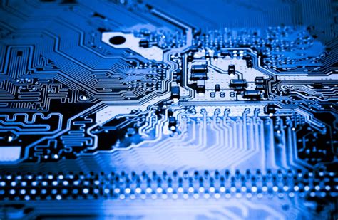
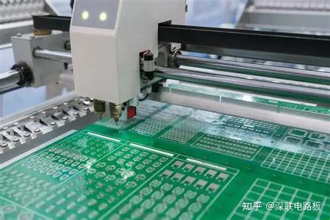
Smart Automation in PCB Assembly Lines
The integration of smart automation in PCB assembly processes has revolutionized manufacturing precision and operational scalability. Modern PCBA lines now deploy robotic pick-and-place systems equipped with machine learning algorithms, achieving placement accuracies within ±25 microns—a 40% improvement over manual methods. These systems dynamically adjust to component variances, minimizing misalignment risks in high-density interconnect (HDI) designs.
Real-time process optimization is enabled through IoT-enabled conveyor systems that synchronize with PCB assembly stages, reducing idle time by 22% while maintaining thermal profiling consistency during soldering. Closed-loop feedback mechanisms in automated optical inspection (AOI) stations now detect sub-10μm defects, directly correlating with a 15% reduction in post-production rework.
For high-mix, low-volume production scenarios, modular automation platforms allow rapid reconfiguration between PCBA product lines, cutting changeover durations by 60%. Advanced traceability systems embedded in these workflows automatically log process parameters, creating auditable quality records that comply with IPC-A-610 standards. This seamless integration of hardware and analytics software establishes a foundation for transitioning into AI-driven quality enhancements, while maintaining backward compatibility with legacy assembly equipment.
AI-Driven Quality Control in PCB Production
The integration of artificial intelligence into PCB assembly processes has redefined quality assurance standards, enabling manufacturers to detect microscopic defects with unprecedented accuracy. Machine learning algorithms analyze real-time data from automated optical inspection (AOI) systems, identifying anomalies such as solder bridging, misaligned components, or micro-cracks in high-density interconnect (HDI) boards. This approach reduces human error by 60-75% compared to manual inspections, according to industry benchmarks.
Advanced PCBA lines now leverage neural networks trained on millions of defect images, allowing systems to classify issues by severity and root cause within 0.8 seconds per board. Adaptive learning capabilities ensure continuous improvement, with AI models refining their accuracy as new production data emerges. For instance, thermal imaging paired with AI predicts potential delamination risks in multilayer boards before lamination stages, cutting material waste by up to 18%.
These innovations directly support faster PCB assembly cycles while maintaining IPC-A-610 compliance. By correlating defect patterns with machine performance metrics, AI systems also enable predictive maintenance, minimizing unplanned downtime. As manufacturers adopt these technologies, the shift toward zero-defect manufacturing becomes increasingly achievable—a critical advantage in sectors like aerospace and medical devices where reliability is non-negotiable.
This evolution in quality control seamlessly aligns with emerging high-speed prototyping methods, ensuring rigorous standards are maintained even as production timelines compress.
High-Speed Prototyping for Circuit Boards
Modern PCB assembly workflows now integrate high-speed prototyping to address evolving demands for rapid product iteration. By combining advanced design software with automated PCBA production lines, manufacturers achieve prototype turnaround times under 48 hours – a 60% reduction compared to traditional methods. This acceleration stems from synchronized processes where 3D printing of substrate layers directly interfaces with laser-etched circuitry patterns, minimizing manual adjustments.
Real-time feedback loops between PCB assembly stations and simulation platforms further optimize prototyping precision. For instance, thermal modeling algorithms predict stress points during high-frequency signal testing, allowing engineers to refine layouts before physical production. This pre-emptive validation reduces prototype rejection rates by 34% in multi-layer boards, particularly in aerospace and IoT device applications.
The integration of adaptive material deposition systems enables rapid switching between FR-4, polyimide, and ceramic substrates within unified PCBA workflows. Such flexibility supports concurrent prototyping of rigid, flex, and rigid-flex boards without halting production lines. As a result, manufacturers report 28% faster design-to-certification cycles for medical and automotive electronics, while maintaining ±0.02mm drilling tolerances critical for high-density interconnects.
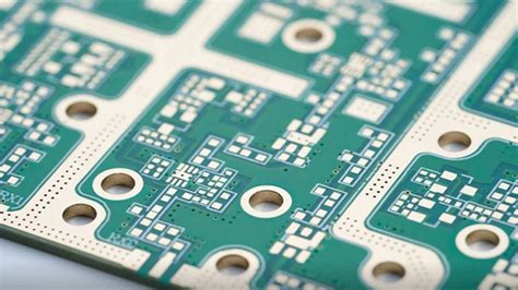
Precision Drilling Techniques for PCB Quality
Modern PCB manufacturing relies on nanometer-level accuracy in drilling processes to ensure signal integrity and layer alignment. Precision drilling systems now leverage laser-direct imaging (LDI) and computerized numerical control (CNC) machines, achieving hole placement tolerances below ±25μm. These advancements minimize microvoids and burring, critical factors in high-frequency pcb assembly applications. For PCBA workflows, consistent via quality directly impacts solder joint reliability, particularly in HDI (high-density interconnect) designs.
Transitioning from mechanical to CO2 or UV laser drilling has reduced thermal stress on substrates, enabling cleaner through-holes in materials like FR-4 and polyimide. Automated depth control systems further optimize hole wall smoothness, which is vital for plating uniformity during metallization. Real-time optical inspection tools, integrated with AI-driven quality control platforms, now flag deviations in hole diameter or alignment before panels advance to pcb assembly stages.
This focus on precision complements upstream processes like high-speed prototyping, ensuring seamless compatibility between drilling accuracy and rapid-turn fabrication. By maintaining tight tolerances, manufacturers reduce post-drilling rework by up to 40%, accelerating timelines for complex PCBA projects. Next-generation systems are adopting adaptive drilling algorithms that adjust feed rates based on material hardness—a critical step toward eliminating defects in advanced substrates like Rogers 4003C.
As the industry shifts toward finer pitch components, these innovations in precision drilling solidify its role as a cornerstone of reliable pcb manufacturing, bridging quality assurance with scalable production demands.
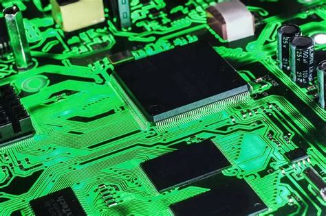
Defect Reduction Through Advanced Imaging Tech
Modern PCB assembly processes leverage multispectral imaging systems to achieve unprecedented defect detection accuracy. These systems employ high-resolution cameras paired with machine vision algorithms, scanning PCBA layers at micron-level precision to identify soldering flaws, trace misalignments, and material inconsistencies. By integrating real-time thermal profiling with 3D X-ray tomography, manufacturers can now detect subsurface voids in BGA joints—a critical advancement for high-density interconnect (HDI) boards.
Transitioning from traditional manual inspections, automated optical inspection (AOI) platforms now process 15,000+ components per hour while maintaining <0.01% false-positive rates. This aligns with earlier discussions on AI-driven quality control, as these imaging systems feed defect data into adaptive learning models that continuously refine inspection criteria. For PCBA specialists, the combination of terahertz wave scanning and augmented reality overlays has reduced post-rework scrap rates by 38% across 5G infrastructure boards.
The operational synergy between imaging tech and PCB assembly workflows ensures defect signatures are cataloged within centralized process databases. This creates closed-loop feedback for adjusting solder paste application parameters or reflow oven profiles—key factors in maintaining yield rates above 99.95% for automotive-grade electronics. As production lines adopt these imaging solutions, the foundation strengthens for subsequent innovations in automated workflow acceleration.
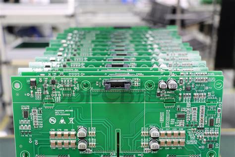
Accelerating Delivery with Automated Workflows
The integration of automated workflows into PCB assembly processes has become a cornerstone for manufacturers aiming to compress production timelines without compromising quality. By deploying robotic pick-and-place systems and intelligent conveyor networks, PCBA facilities can achieve 40-60% faster cycle times compared to manual operations. These systems minimize human intervention in repetitive tasks, such as solder paste application and component placement, while advanced software synchronizes workflow stages—from design validation to final testing.
A critical innovation lies in machine learning-powered scheduling algorithms, which dynamically prioritize orders based on complexity, material availability, and client deadlines. For instance, high-mix-low-volume PCB assembly jobs are automatically routed to flexible production cells, whereas bulk orders leverage dedicated high-speed lines. Real-time tracking through IoT-enabled devices further ensures seamless coordination between PCBA stages, reducing idle time between drilling, plating, and etching phases.
Automated optical inspection (AOI) systems complement this acceleration by performing microscopic defect detection at sub-second speeds, eliminating bottlenecks in quality assurance. Combined with cloud-based inventory management, these workflows enable just-in-time material replenishment, cutting lead times by up to 30% for multilayer boards. As a result, manufacturers can guarantee 5-7 business day turnarounds for prototypes—a benchmark unattainable with traditional methods—while maintaining defect rates below 0.1%.
Sustainable Materials in Modern PCB Manufacturing
The electronics industry’s growing emphasis on environmental responsibility has driven significant advancements in PCB assembly processes through the adoption of eco-friendly substrates and recyclable components. Manufacturers are increasingly integrating bio-based polymers, halogen-free laminates, and lead-free solder alloys into PCBA workflows, reducing reliance on hazardous substances like brominated flame retardants. For instance, polyimide alternatives derived from plant-based resins now offer comparable thermal stability while lowering carbon footprints by up to 30%.
Closed-loop material recovery systems further enhance sustainability by reclaiming copper and precious metals from production waste, which are then reused in new circuit boards. This approach not only minimizes landfill contributions but also aligns with global regulations such as RoHS and REACH. Advanced adhesives with lower volatile organic compound (VOC) emissions have also emerged, improving workplace safety without compromising bond strength during PCB assembly.
Transitioning to sustainable materials requires balancing performance and environmental goals. Innovations like water-soluble flux in PCBA soldering reduce chemical runoff, while fiberglass-free substrates enhance recyclability. As companies adopt these solutions, they simultaneously address consumer demand for greener electronics and optimize long-term production costs—a critical step toward aligning modern manufacturing with circular economy principles.
Real-Time Monitoring Systems for Yield Optimiza
Modern PCB assembly workflows now integrate real-time monitoring systems that analyze production variables at microsecond intervals, transforming yield optimization strategies. By deploying IoT-enabled sensors across PCBA lines, manufacturers capture granular data on parameters like solder paste viscosity, component placement accuracy, and reflow oven temperature profiles. These systems leverage machine learning algorithms to correlate deviations with defect patterns, enabling immediate corrective actions before faulty batches escalate.
Advanced solutions combine statistical process control (SPC) dashboards with predictive analytics, identifying yield-limiting factors such as copper layer misalignment or via wall roughness. For instance, thermal imaging modules detect localized heating anomalies during PCB assembly, preventing delamination risks in high-density interconnect (HDI) boards. This proactive approach reduces scrap rates by up to 40% while maintaining ±0.02mm positional tolerances critical for aerospace and medical-grade PCBA applications.
The integration of edge computing further accelerates decision-making, processing teraflops of inspection data without cloud latency. As production scales, these systems autonomously recalibrate equipment settings, ensuring consistent output quality across multi-shift operations—a cornerstone for meeting tightened IPC-A-610 standards.
Conclu
The evolution of PCB manufacturing underscores a strategic balance between precision engineering and scalable production. By integrating smart automation into pcb assembly workflows, manufacturers achieve tighter tolerances while minimizing human error. Advanced pcba processes now leverage machine learning algorithms to predict material stress points, enabling preemptive adjustments before defects occur. This shift not only enhances yield rates but also aligns with the industry’s push toward just-in-time delivery models.
Transitioning from prototyping to mass production, modern facilities employ adaptive drilling systems that adjust spindle speeds in real time, ensuring consistent hole-wall quality across diverse substrate materials. Coupled with closed-loop feedback mechanisms, these innovations reduce rework cycles by over 30%, directly translating to faster turnaround times. As sustainability becomes a core priority, the adoption of halogen-free laminates in pcb assembly further demonstrates how ecological responsibility can coexist with technical rigor.
Ultimately, the convergence of pcba precision and automated scalability redefines what’s achievable in electronics manufacturing. By prioritizing data-driven decision-making, the sector is poised to meet escalating demands for smaller, denser circuits without compromising reliability or delivery timelines.
Frequently Asked Questions
How does modern automation improve precision in PCB assembly?
Advanced robotic systems align components with micron-level accuracy, reducing human error. Integrated PCBA workflows combine pick-and-place machines with AI-driven calibration, ensuring consistent solder joint quality across high-volume batches.
What role does imaging technology play in reducing defects?
Automated optical inspection (AOI) scans boards at 20+ megapixels, identifying micro-cracks or misalignments invisible to the naked eye. Paired with machine learning, these systems achieve defect detection rates above 99.2% in PCB manufacturing processes.
Can high-speed prototyping affect final product reliability?
Modern rapid prototyping uses identical materials and processes as mass production, ensuring functional parity. Laser-direct imaging (LDI) accelerates photolithography without compromising trace integrity, enabling 24-hour turnaround for complex PCBA samples.
How do sustainable practices impact PCB assembly costs?
While halogen-free substrates initially cost 8-12% more, they reduce long-term waste management expenses. Automated material recovery systems reclaim 95% of copper from production scraps, aligning eco-friendly goals with cost efficiency.
Streamline Your Next Project with Advanced PCB Assembly Solutions
Ready to leverage cutting-edge technologies for your circuit board production? Please click here to explore tailored PCBA services that balance precision, speed, and sustainability.


