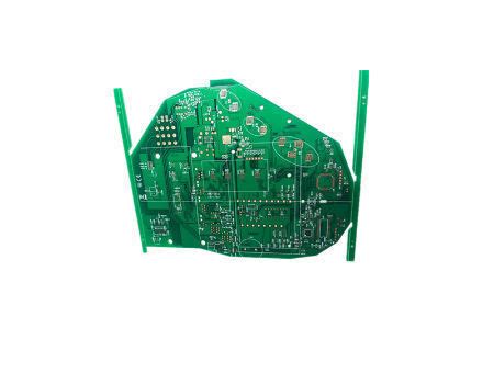
Building High-Quality PCBs: Assembly Essentials
Key Takeaways
Successful PCB assembly (PCBA) relies on a combination of technical precision and methodical planning. Below are critical insights to ensure high-quality results:
Mastering PCB Soldering Techniques
Proper soldering ensures electrical stability. Use temperature-controlled irons to avoid thermal damage, and apply flux to minimize oxidation. For surface-mount components, reflow soldering is preferred for consistency.Component Placement Best Practices
Organize components by size and function to streamline workflows. Always follow the design schematic to prevent misalignment, and use automated pick-and-place machines for high-volume projects.
Tip: "Cleanliness is non-negotiable. Dust or residue can compromise solder joints—use an anti-static brush during placement."
| Factor | Traditional Assembly | Modern PCBA |
|---|---|---|
| Soldering Method | Manual iron | Reflow oven |
| Component Density | Low to moderate | High (microcomponents) |
| Error Rate | 8-12% | <3% (with automation) |
Essential PCB Quality Testing Methods
Incorporate automated optical inspection (AOI) to detect soldering defects and in-circuit testing (ICT) for electrical validation. Functional testing under real-world conditions ensures reliability.Avoiding Common PCB Assembly Errors
Misaligned components, cold solder joints, and electrostatic discharge (ESD) are frequent pitfalls. Implement grounding straps and adhere to IPC-A-610 standards for compliance.
By integrating these principles, PCB assembly workflows achieve higher yields, reduced rework, and enhanced product longevity. Focus on precision tools, rigorous testing, and adherence to industry benchmarks to optimize PCBA outcomes.
Mastering PCB Soldering Techniques
Effective soldering is the backbone of reliable PCB assembly, requiring a balance of precision, temperature control, and material selection. Whether using hand soldering for prototypes or reflow ovens for high-volume PCBA, understanding thermal profiles is critical. For instance, lead-based solder typically melts at 183°C (361°F), while lead-free alternatives require temperatures above 217°C (422°F). Overheating can damage components, while insufficient heat risks cold joints—a common flaw that weakens electrical connections.
To ensure consistency, maintain a clean workspace and use flux to eliminate oxidation. For surface-mount devices (SMDs), align components accurately before soldering, as misplacement often leads to signal interference or short circuits. Inspect joints under magnification: ideal connections appear smooth and concave, not dull or lumpy. Automated optical inspection (AOI) systems in PCBA workflows can detect microscopic defects, but manual verification remains valuable for complex boards.
When transitioning between soldering methods, consider the thermal mass of components—larger parts dissipate heat faster, requiring adjusted iron settings. Finally, always test solder joints with a multimeter to confirm conductivity. By mastering these techniques, you lay the foundation for durable PCB assembly and minimize post-production troubleshooting.
Component Placement Best Practices
Effective PCB assembly relies on meticulous component placement to ensure electrical functionality and mechanical stability. Begin by analyzing the design layout to prioritize critical components, such as microcontrollers or power regulators, positioning them to minimize signal interference and thermal buildup. Maintain 3-5mm clearance between heat-sensitive parts and high-temperature elements like voltage regulators, using thermal relief pads where necessary.
When placing surface-mount devices (SMDs), align solder pads precisely with component terminals to prevent tombstoning or skewed connections during reflow soldering. For through-hole components, verify hole diameters match lead sizes to avoid loose fits or solder bridging. Automated PCBA processes benefit from standardized orientation—align all polarized components (e.g., diodes, capacitors) uniformly to streamline inspection and troubleshooting.
Group related functional blocks together, such as power supply circuits or RF modules, to reduce trace lengths and electromagnetic interference. Adhere to Design for Manufacturing (DFM) guidelines, ensuring adequate spacing for pick-and-place machinery and rework tools. Double-check component footprints against the bill of materials (BOM) to prevent mismatches, a common source of assembly delays.
By optimizing placement strategies, PCB assembly workflows achieve higher yield rates while supporting rigorous quality testing phases. This foundational step directly impacts the board’s durability, signal integrity, and compliance with industry standards.
Essential PCB Quality Testing Methods
Effective PCB assembly requires rigorous quality control to ensure reliability and functionality. Following meticulous soldering and component placement, PCBA validation begins with automated optical inspection (AOI). This non-contact method scans boards for defects like solder bridges, misaligned components, or insufficient solder joints. For hidden connections, X-ray inspection analyzes ball grid arrays (BGAs) and via integrity, critical for high-density designs.
In-circuit testing (ICT) evaluates electrical performance by verifying resistance, capacitance, and voltage levels against design specifications. Combined with functional testing—simulating real-world operating conditions—this ensures signal integrity and thermal stability. Environmental stress tests, such as thermal cycling or vibration testing, further validate PCB durability under extreme conditions.
To minimize human error, modern PCBA workflows integrate statistical process control (SPC) tools, tracking defect rates and refining assembly parameters. Prioritizing these methods reduces field failures and aligns with industry standards like IPC-A-610 or ISO 9001. By balancing automated precision with targeted manual checks, manufacturers achieve zero-defect benchmarks while optimizing production timelines.
Avoiding Common PCB Assembly Errors
Even experienced technicians can encounter pitfalls during PCB assembly if critical steps are overlooked. One frequent mistake involves solder bridging, where excess solder creates unintended connections between adjacent pads. This often occurs in high-density PCBA designs, emphasizing the need for precise temperature control and calibrated soldering equipment. Another common error is component misalignment, particularly with surface-mount devices (SMDs). Using automated optical inspection (AOI) systems helps verify placement accuracy before permanent soldering.
Improper handling of moisture-sensitive components can also compromise reliability. For example, integrated circuits (ICs) exposed to ambient humidity without pre-bake protocols may suffer from popcorning during reflow. Additionally, neglecting PCB assembly cleanliness—such as residual flux left on boards—can lead to corrosion or electrical shorts over time. Implementing thorough post-solder cleaning processes mitigates this risk.
Design-related oversights, like inadequate thermal relief in copper pours, may cause uneven heating during soldering, resulting in weak joints. Always validate design files against PCBA manufacturing guidelines to avoid rework. Finally, skipping functional testing after assembly—such as in-circuit testing (ICT) or boundary scan—risks shipping defective units. Integrating real-time quality checks at multiple stages ensures errors are caught early, reducing costly delays. By addressing these pitfalls systematically, manufacturers can enhance yield rates and maintain consistent product performance.
Optimizing PCB Durability & Performance
Achieving long-term reliability in PCB assembly requires a strategic focus on material selection, thermal management, and environmental resilience. Start by choosing substrate materials like FR4 or polyimide based on operational demands—high-temperature environments benefit from glass transition temperatures (Tg) above 170°C. For PCBA designs, ensure proper thermal via placement and copper weight distribution to dissipate heat efficiently, minimizing stress on sensitive components.
Mechanical stability is equally critical. Secure components using adhesive underfills or conformal coatings to protect against vibration and moisture ingress. Implement design-for-manufacturing (DFM) principles, such as maintaining adequate trace widths and spacing, to prevent solder bridging or micro-cracks during thermal cycling.
Performance optimization hinges on rigorous testing protocols. Use automated optical inspection (AOI) and X-ray analysis to detect latent defects in PCB assembly, while environmental stress screening (ESS) validates durability under extreme conditions. For high-frequency applications, prioritize impedance-controlled routing and shield critical traces to reduce electromagnetic interference (EMI).
Finally, collaborate closely with PCBA suppliers to align material specs with performance goals, ensuring compatibility between components and soldering alloys. By balancing these factors, engineers can enhance both the lifespan and functionality of assembled boards, even in demanding applications.
Step-by-Step PCB Assembly Guide
A systematic approach ensures consistent results in PCB assembly, whether producing prototypes or full-scale PCBA batches. Begin by preparing all components, solder materials, and design files, verifying that the bill of materials (BOM) matches the schematic layout. Stencil printers then apply solder paste to designated pads, requiring precise alignment to avoid bridging or insufficient coverage.
Next, pick-and-place machines or manual tweezers position components according to the assembly diagram, prioritizing sensitive parts like ICs or connectors. Double-check orientations—incorrectly placed diodes or polarized capacitors account for over 30% of early-stage defects. The board then enters a reflow oven, where controlled heating profiles melt solder paste, forming secure electrical connections.
Post-soldering, inspect joints using automated optical inspection (AOI) or magnification tools, identifying cold joints or tombstoning. Functional testing follows, where power-up sequences and signal integrity checks validate the PCBA’s performance. For complex boards, X-ray inspection detects hidden flaws in ball grid arrays (BGAs) or under components.
Finally, apply conformal coatings or mechanical housings if required, ensuring environmental resilience. Document each stage meticulously, as traceability streamlines troubleshooting and future optimizations. By adhering to this workflow, manufacturers balance speed with precision, minimizing rework and maximizing PCB durability.
Troubleshooting PCB Assembly Issues
Even with meticulous planning, challenges can arise during PCB assembly that compromise functionality. Identifying the root cause requires a systematic approach, beginning with visual inspections for obvious defects like cold joints or misaligned components. For intermittent failures, thermal imaging can reveal overheating areas, while X-ray inspection helps detect hidden issues such as internal shorts or voids in solder joints under BGAs.
Common PCBA errors often stem from soldering inconsistencies—whether excessive solder causing bridging or insufficient heat leading to weak connections. Reflow profile deviations, such as incorrect ramp rates or peak temperatures, account for over 30% of manufacturing defects. Always cross-verify solder paste specifications and stencil alignment to prevent footprint mismatches.
When troubleshooting signal integrity problems, use oscilloscopes to trace noise sources or impedance mismatches, particularly in high-frequency circuits. For persistent electrical failures, isolate sections of the board and test individually to pinpoint faulty components or traces.
Documentation is critical: maintain detailed records of PCB assembly stages, including paste application, component placement, and reflow parameters. This practice accelerates defect correlation and supports root cause analysis. Finally, validate fixes through functional testing and environmental stress tests to ensure reliability under operational conditions.
By integrating these strategies, teams can reduce rework cycles by up to 45% while enhancing PCBA quality—a crucial step before advancing to final performance optimization phases.
Pro Tips for Precision PCB Assembly
Achieving flawless PCB assembly requires a blend of technical expertise and meticulous attention to detail. Start by ensuring thermal management is prioritized during soldering—uneven heat distribution can warp boards or weaken joints. Use a preheating stage to gradually elevate temperatures, minimizing stress on sensitive components. For PCBA workflows, invest in high-quality stencils to guarantee consistent solder paste application, reducing the risk of bridging or insufficient connections.
Another often overlooked factor is component orientation. Align polarized parts uniformly to simplify automated inspection and avoid misplacement during reflow. When handling fine-pitch ICs or micro-BGA packages, employ vacuum pens or tweezers with anti-static coatings to prevent physical or electrostatic damage. For manual adjustments, verify solder joint integrity under magnification—microscopic cracks or cold joints can compromise long-term reliability.
Incorporate torque-controlled tools for mechanical fasteners to avoid over-tightening, which may fracture boards or stress solder points. Implementing environmental controls, such as humidity-stable workspaces, further mitigates risks like oxidation or moisture absorption. Finally, validate every PCBA batch with in-process testing, combining automated optical inspection (AOI) and X-ray imaging to detect hidden defects. By refining these practices, assemblers can consistently deliver precision-engineered boards that meet rigorous performance standards.
Conclusion
Successful PCB assembly hinges on balancing technical precision with systematic quality control. From meticulous soldering techniques to strategic component placement, each step directly impacts the reliability of the final PCBA. Rigorous quality testing, including automated optical inspection (AOI) and functional testing, ensures defects are identified early, minimizing costly rework. By adhering to industry standards and leveraging modern tools like pick-and-place machines, manufacturers can optimize thermal management and signal integrity—key factors in enhancing PCB durability and performance.
Furthermore, avoiding common errors, such as solder bridging or misaligned components, requires continuous training and adherence to documented workflows. Implementing thorough design-for-manufacturing (DFM) checks prior to production further streamlines the assembly process. Whether prototyping or scaling production, prioritizing precision at every stage transforms complex designs into robust, functional boards. Ultimately, a disciplined approach to PCB assembly not only reduces failure rates but also extends the lifespan of electronic devices, reinforcing the importance of mastering these essential practices.
FAQs
What is the difference between PCB assembly and PCBA?
PCB assembly refers to the process of attaching electronic components to a printed circuit board, while PCBA (Printed Circuit Board Assembly) denotes the completed board with all components installed. Both terms are often used interchangeably, but PCBA emphasizes the finished product.
How can I avoid solder bridging during assembly?
To prevent solder bridging, ensure precise temperature control during reflow soldering and use solder masks. Proper stencil alignment and adequate spacing between pads also minimize unintended connections.
Why is thermal management critical in PCB assembly?
Thermal stress from soldering or component operation can warp boards or damage parts. Implementing thermal relief pads and selecting materials with suitable heat tolerance optimizes durability in PCBA designs.
What tools are essential for quality testing?
Automated Optical Inspection (AOI) systems, multimeters, and X-ray inspection tools are vital. These identify cold joints, misaligned components, or shorts, ensuring reliability in PCB assembly workflows.
How do I choose between manual and automated PCBA methods?
Manual assembly suits low-volume, high-mix projects requiring flexibility. Automated lines excel in high-volume production, ensuring consistency and speed. Evaluate cost, volume, and complexity to decide.
Ready to Optimize Your PCB Assembly Process?
For expert guidance on PCB assembly or custom PCBA solutions, please click here to connect with our engineering team.


