Calculating the Resistance of PCB Traces: A Comprehensive Guide
Introduction
Printed Circuit Board (PCB) trace resistance calculation is a fundamental skill for electronics designers and engineers. Understanding how to accurately determine the resistance of copper traces on a PCB is essential for proper power distribution, signal integrity analysis, and thermal management. This article provides a detailed examination of the methods and considerations involved in calculating PCB trace resistance.
1. Basic Principles of PCB Trace Resistance
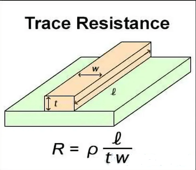
The resistance of a PCB trace follows the same basic principle as any electrical conductor, defined by Ohm’s Law:
R = ρ × (L / A)
Where:
- R = Resistance in ohms (Ω)
- ρ (rho) = Resistivity of the material (Ω·m)
- L = Length of the conductor (m)
- A = Cross-sectional area of the conductor (m²)
For PCB traces, we typically use:
- Copper resistivity (ρ) = 1.72 × 10⁻⁸ Ω·m (at 20°C)
- Length (L) in meters or more commonly in inches/cm
- Cross-sectional area (A) = thickness (t) × width (w)
2. Key Parameters Affecting PCB Trace Resistance
2.1 Copper Thickness
PCB copper thickness is typically specified in ounces (oz), where 1 oz copper means 1 ounce of copper per square foot, which equates to approximately 1.37 mils (34.79 μm) thickness.
Common copper weights:
- 0.5 oz = 0.685 mils (17.4 μm)
- 1 oz = 1.37 mils (34.8 μm)
- 2 oz = 2.74 mils (69.6 μm)
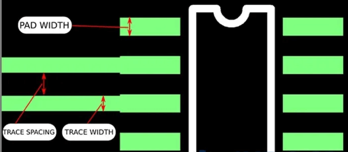
2.2 Trace Width and Length
The width and length of the trace directly affect resistance:
- Wider traces have lower resistance
- Longer traces have higher resistance
2.3 Temperature Effects
Copper resistivity increases with temperature:
ρ(T) = ρ₀[1 + α(T – T₀)]
Where:
- ρ₀ = resistivity at reference temperature T₀ (typically 20°C)
- α = temperature coefficient of copper (0.00393/°C)
- T = actual temperature (°C)
3. Practical Calculation Methods
3.1 Basic DC Resistance Calculation
For a straight trace with uniform cross-section:
R = ρ × (L / (t × w))
Where:
- ρ = 1.72 × 10⁻⁸ Ω·m (copper)
- L = length in meters
- t = thickness in meters
- w = width in meters
Example calculation:
- 1 oz copper (34.79 μm)
- Trace width: 10 mils (0.254 mm)
- Trace length: 1 inch (25.4 mm)
Convert all to meters:
t = 34.79 × 10⁻⁶ m
w = 0.254 × 10⁻³ m
L = 25.4 × 10⁻³ m
R = (1.72 × 10⁻⁸) × (25.4 × 10⁻³) / (34.79 × 10⁻⁶ × 0.254 × 10⁻³)
= 1.72 × 10⁻⁸ × 25.4 × 10⁻³ / (8.84 × 10⁻⁹)
= 4.94 × 10⁻⁷ Ω
This seems incorrect – let’s use more practical units:
3.2 Simplified Calculation Using Common Units
A more practical formula using common PCB units:
R = (ρ × L) / (t × w) × C
Where:
- ρ = 6.787 × 10⁻⁷ Ω·in (copper resistivity in ohms per inch)
- L = length in inches
- t = thickness in inches
- w = width in inches
- C = unit correction factor (1 for inches)
For our previous example:
1 oz copper = 0.00137 in
Width = 0.010 in
Length = 1 in
R = (6.787 × 10⁻⁷ × 1) / (0.00137 × 0.010)
= 6.787 × 10⁻⁷ / 1.37 × 10⁻⁵
= 0.0495 Ω or 49.5 mΩ
3.3 Resistance per Unit Length
A useful metric is resistance per unit length (e.g., ohms per inch):
R/inch = ρ / (t × w)
For 1 oz copper (t=0.00137 in):
R/inch = 6.787 × 10⁻⁷ / (0.00137 × w)
= 4.954 × 10⁻⁴ / w (where w is in inches)
For our 10 mil (0.010 in) trace:
R/inch = 4.954 × 10⁻⁴ / 0.010 = 0.0495 Ω/inch
3.4 Using PCB Resistance Calculators
Many online calculators and PCB design tools can automatically calculate trace resistance by inputting:
- Copper weight (oz)
- Trace width
- Trace length
- Temperature
These tools incorporate the resistivity values and unit conversions automatically.
4. Advanced Considerations
4.1 AC Resistance and Skin Effect
At high frequencies (>10 MHz), current tends to flow near the surface of the conductor (skin effect), increasing effective resistance.
Skin depth (δ) is calculated as:
δ = √(ρ / (π × μ × f))
Where:
- μ = permeability of copper (4π × 10⁻⁷ H/m)
- f = frequency (Hz)
The effective AC resistance becomes:
R_ac ≈ R_dc × (t / (2δ)) for t > δ
4.2 Non-Uniform Traces
For non-rectangular traces or those with variations:
- Divide into segments with uniform cross-sections
- Calculate resistance for each segment
- Sum the resistances
4.3 Via Resistance
Vias contribute additional resistance:
R_via ≈ ρ × (h / (π × r²))
Where:
- h = via height (length)
- r = via radius
4.4 Surface Roughness
High-frequency signals are affected by copper surface roughness, which can increase effective resistance by 10-50%.
5. Practical Examples
Example 1: Power Distribution Trace
Calculate resistance of a 5V power trace:
- 2 oz copper
- Width: 50 mils (0.050 in)
- Length: 6 inches
R/inch for 2 oz = (6.787 × 10⁻⁷) / (0.00274 × w)
= 2.477 × 10⁻⁴ / w
For w = 0.050 in:
R/inch = 2.477 × 10⁻⁴ / 0.050 = 0.00495 Ω/inch
For 6 inches:
R_total = 6 × 0.00495 = 0.0297 Ω
Example 2: High-Frequency Signal Trace
Calculate DC and 1 GHz AC resistance for:
- 1 oz copper
- Width: 8 mils (0.008 in)
- Length: 3 inches
DC resistance:
R/inch = 4.954 × 10⁻⁴ / 0.008 = 0.0619 Ω/inch
R_total = 3 × 0.0619 = 0.186 Ω
AC resistance at 1 GHz:
Skin depth (δ) = √(1.72 × 10⁻⁸ / (π × 4π × 10⁻⁷ × 1 × 10⁹))
= 2.09 μm = 0.082 mils
1 oz copper thickness = 1.37 mils > 2δ, so skin effect applies
R_ac ≈ R_dc × (t / (2δ)) = 0.186 × (1.37 / (2 × 0.082)) ≈ 1.55 Ω
6. Mitigation Strategies for High Resistance
When trace resistance is too high:
- Increase copper weight (2 oz instead of 1 oz)
- Widen the trace
- Shorten the trace length
- Use multiple parallel traces
- Add power/ground planes for return paths
- For high frequencies, consider surface finish effects
7. Tools and Resources
Several tools can assist with PCB trace resistance calculations:
- Online calculators (Saturn PCB Toolkit, EEWeb, etc.)
- PCB design software with integrated analysis (Altium, Cadence, etc.)
- Spreadsheet-based calculators
- MATLAB/Python scripts for custom calculations
Conclusion
Accurate calculation of PCB trace resistance is essential for successful electronic design. By understanding the fundamental principles, key parameters, and practical calculation methods, designers can ensure proper power delivery, minimize signal degradation, and prevent thermal issues. While basic DC resistance calculations are straightforward, advanced applications require consideration of frequency effects, temperature variations, and physical trace characteristics. Modern PCB design tools incorporate many of these calculations, but a solid understanding of the underlying principles remains invaluable for troubleshooting and optimization.
Remember that trace resistance is just one factor in overall PCB performance – it must be considered alongside capacitance, inductance, and the specific requirements of your application. With practice, resistance calculations become second nature, allowing you to make informed design decisions that improve the reliability and performance of your electronic systems.