Castellated PCBs: Design, Applications, and Manufacturing Considerations
Introduction to Castellated PCBs
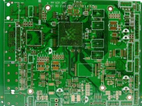
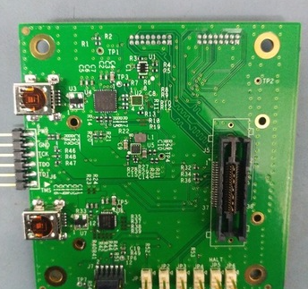
Castellated printed circuit boards (PCBs) represent a specialized design approach that enables modular electronics assembly and simplified board-to-board connections. These unique PCBs feature a series of semi-plated holes or indentations along their edges that resemble the battlements of a castle—hence the name “castellated.” This distinctive edge configuration serves as both a mechanical attachment point and electrical connection interface between multiple circuit boards.
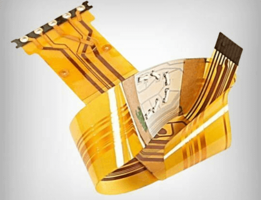
The castellated edge design has gained significant popularity in modern electronics manufacturing due to its space-saving advantages and reliable interconnection capabilities. Unlike traditional connection methods that require separate connectors or complex wiring, castellated PCBs allow for direct soldering of one board to another, creating a compact and robust assembly. This technology has become particularly valuable in applications where miniaturization is critical, such as wearable devices, IoT modules, and compact consumer electronics.
Historical Development and Evolution
The concept of castellated holes in PCBs emerged as engineers sought more efficient ways to connect modular circuit boards without using conventional connectors. Early implementations appeared in the 1990s, primarily in telecommunications equipment where high-density interconnections were required. The technique drew inspiration from castellation processes used in medieval architecture and was adapted to meet the precision requirements of electronic assemblies.
Over time, the design and manufacturing processes for castellated PCBs have evolved significantly. Advancements in PCB fabrication technologies, particularly in precision drilling and plating techniques, have enabled more reliable and consistent castellation production. Modern surface mount technology (SMT) equipment has also adapted to handle these specialized boards, with improved soldering processes ensuring strong, reliable connections between castellated modules.
Design Principles of Castellated PCBs
Basic Structure and Geometry
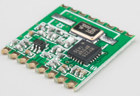
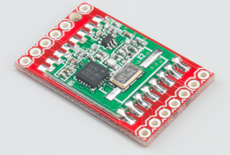
Castellated PCBs feature a series of semi-circular indentations or half-holes along one or more edges of the board. These castellations are created by drilling complete holes at the board edge and then cutting through them during the routing process, leaving half of the plated hole on the board edge. The remaining semicircular pads provide both mechanical anchoring points and electrical connection surfaces.
Standard castellation dimensions typically range from 0.8mm to 1.6mm in diameter, with spacing (pitch) between castellations varying according to application requirements. The plating of these half-holes usually extends across the entire edge surface, ensuring good electrical conductivity and solderability. Designers must carefully consider the relationship between castellation size, board thickness, and the required mechanical strength of the final assembly.
Key Design Considerations
Several critical factors influence the design of effective castellated PCBs:
- Board Material Selection: The choice of substrate material (typically FR-4, but sometimes high-frequency or flexible materials) affects both the mechanical stability of the castellations and their electrical performance.
- Copper Plating Thickness: Adequate copper plating in the castellations ensures reliable electrical connections and sufficient solder joint strength. A minimum plating thickness of 25μm is generally recommended.
- Solder Mask and Surface Finish: Appropriate solder mask application prevents solder bridging between adjacent castellations, while surface finishes like ENIG (Electroless Nickel Immersion Gold) or HASL (Hot Air Solder Leveling) enhance solderability.
- Thermal Management: Designers must account for heat dissipation, especially when castellated boards are used in high-power applications, as the connection points can affect thermal pathways.
- Mechanical Stress Distribution: The layout should distribute mechanical stresses evenly across multiple castellations to prevent concentration at single points that could lead to failure.
Manufacturing Process
Fabrication Steps
The production of castellated PCBs follows a specialized sequence within the standard PCB manufacturing workflow:
- Drilling Complete Holes: Standard through-holes are drilled at the future board edges where castellations will be located.
- Plating Process: The holes undergo standard plating procedures, creating conductive barrels that will become the castellations.
- Routing/Cutting: The board is routed precisely through the center of the plated holes, creating the characteristic half-hole castellations.
- Edge Quality Control: Special attention is given to ensuring clean, burr-free edges on the castellations to facilitate proper soldering.
- Surface Finishing: The final surface finish is applied to protect the exposed copper and enhance solderability.
Quality Assurance Measures
Manufacturers implement several quality control measures specific to castellated PCBs:
- Microscopic inspection of castellation edges to verify plating integrity
- Solderability testing to ensure proper wetting characteristics
- Dimensional verification using precision measurement tools
- Cross-section analysis of sample castellations to confirm plating thickness and uniformity
Applications and Use Cases
Common Implementation Scenarios
Castellated PCBs find application in numerous electronic products and systems:
- Module-on-Board Assemblies: Many wireless modules (Wi-Fi, Bluetooth, cellular) use castellated edges for direct attachment to main system boards.
- Stacked PCB Configurations: Multiple boards can be vertically interconnected using castellated edges to create compact three-dimensional assemblies.
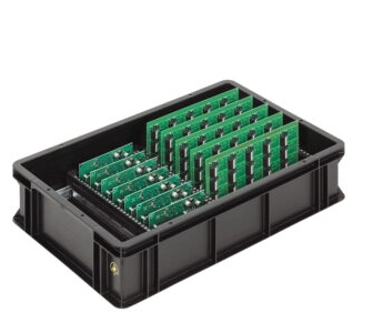
- Breakaway Board Designs: Some manufacturers produce multiple PCBs as a single panel with castellated edges for easy separation after assembly.
- Test and Programming Fixtures: Castellated edges allow temporary attachment of test interfaces that can be removed after programming or validation.
Industry-Specific Applications
Various industries leverage castellated PCB technology for specific advantages:
- Consumer Electronics: Smartphones, tablets, and wearables use castellated modules to save space and simplify assembly.
- Automotive Electronics: Control modules often employ castellated designs for reliable connections in vibration-prone environments.
- Industrial Equipment: Sensor modules and control interfaces benefit from the robust connections provided by castellations.
- Medical Devices: Compact medical monitors and implantable devices utilize castellated designs for miniaturization.
Advantages of Castellated PCBs
Space Efficiency and Miniaturization
One of the primary benefits of castellated PCBs is their ability to save valuable board space. By eliminating the need for separate connectors, designers can reduce the overall footprint of electronic assemblies. This advantage is particularly crucial in portable and wearable devices where every millimeter counts.
Cost Reduction Factors
Castellated designs offer several cost-saving aspects:
- Elimination of separate connector components
- Reduction in assembly steps compared to connector-based approaches
- Lower inventory costs due to fewer distinct parts
- Potential for automated assembly processes
Reliability Enhancements
Properly designed castellated connections provide:
- Fewer potential failure points compared to socketed connectors
- Improved resistance to vibration and mechanical shock
- Better electrical performance with shorter signal paths
- Enhanced thermal transfer between boards in some configurations
Challenges and Limitations
Design Constraints
Despite their advantages, castellated PCBs present certain design challenges:
- Limited Repairability: Once soldered, castellated connections can be difficult to rework or replace without potentially damaging the boards.
- Alignment Precision: The assembly process requires precise alignment between mating castellated edges to ensure proper connections.
- Current Carrying Capacity: Each castellation has limited current-carrying capability, potentially requiring multiple parallel connections for high-current applications.
- Signal Integrity Considerations: High-speed signals may require careful routing and grounding when passing through castellated connections.
Manufacturing Complexities
Fabricating high-quality castellated PCBs presents unique production challenges:
- Higher precision requirements in drilling and routing operations
- Increased risk of plating defects at board edges
- Potential for copper tearing during the routing process
- Greater sensitivity to handling damage during manufacturing and assembly
Best Practices for Castellated PCB Design
Layout Guidelines
To maximize the benefits of castellated designs, engineers should follow these recommendations:
- Provide Adequate Spacing: Maintain sufficient clearance between castellations and nearby components or board features.
- Include Fiducial Marks: Incorporate alignment aids to facilitate precise placement during assembly.
- Optimize Castellation Pattern: Arrange castellations to evenly distribute mechanical and electrical loads.
- Consider Thermal Expansion: Account for differences in thermal expansion coefficients between connected boards.
- Implement Proper Grounding: Ensure low-impedance ground connections between boards for optimal signal integrity.
Assembly Recommendations
Successful assembly of castellated PCBs requires attention to several factors:
- Use of appropriate solder paste formulations and stencil designs
- Precise control of soldering temperature profiles
- Proper support and fixturing during the reflow process
- Implementation of inspection procedures to verify solder joint quality
Future Trends and Developments
Emerging Applications
The use of castellated PCBs continues to expand into new areas:
- Ultra-Miniaturized IoT Devices: As IoT nodes shrink, castellated designs enable increasingly compact implementations.
- Flexible Hybrid Electronics: Combinations of rigid and flexible PCBs using castellated interfaces.
- High-Density 3D Packaging: Advanced stacking techniques leveraging castellated connections.
Technological Advancements
Several developments are shaping the future of castellated PCB technology:
- Improved Manufacturing Techniques: Enhanced drilling and routing technologies for more precise castellations.
- Advanced Materials: Adoption of high-performance substrates for better reliability in demanding environments.
- Automated Optical Inspection (AOI): Enhanced inspection systems specifically tuned for castellated connections.
- Design Software Improvements: CAD tools with specialized features for castellated PCB design and verification.
Conclusion
Castellated PCBs represent a sophisticated solution for modern electronics packaging challenges, offering unique advantages in space-constrained applications. Their ability to provide both mechanical attachment and electrical interconnection in a single, compact interface has made them indispensable in numerous industries. While they present certain design and manufacturing challenges, following established best practices can yield highly reliable and cost-effective implementations.
As electronic devices continue to trend toward greater miniaturization and functional integration, the importance of castellated PCB technology is likely to grow. Engineers who master the principles of castellated design will be well-positioned to develop innovative products that meet the evolving demands of the electronics marketplace. With ongoing advancements in materials, manufacturing processes, and design tools, castellated PCBs will remain a vital technology for creating compact, reliable electronic assemblies across diverse applications.