advanced circuits barebones | additive pcb | additive pcb manufacturing | advanced assembly pcb | advanced circuit board | advanced circuits 4pcb | advanced circuits assembly | advanced circuits pcb | advanced pcb manufacturing | advanced printed circuit technology | aerospace pcb assembly
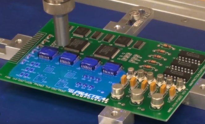
Basic points for PCB component welding
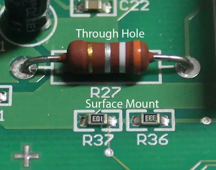
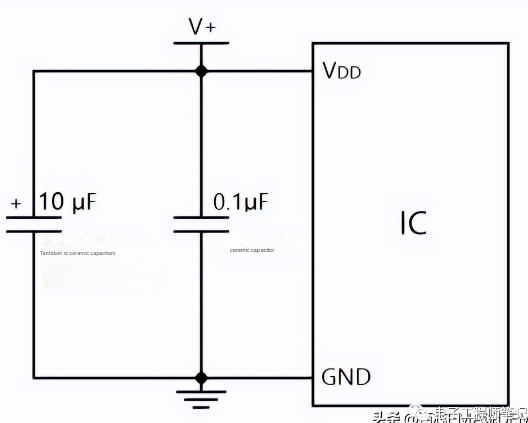
Before welding: During welding: After welding: Soldering specifications for mounted components: