Why PCB Cloning Has Fallen into a Dilemma: A Comprehensive Analysis
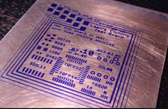
Introduction Printed Circuit Board (PCB) cloning, also known as PCB copying or reverse engineering, has long been a controversial practice…
Blogs
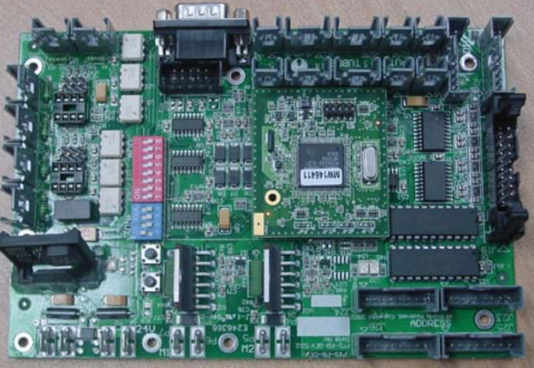
Introduction Printed Circuit Board (PCB) cloning, also known as PCB copying or reverse engineering, has long been a controversial practice…
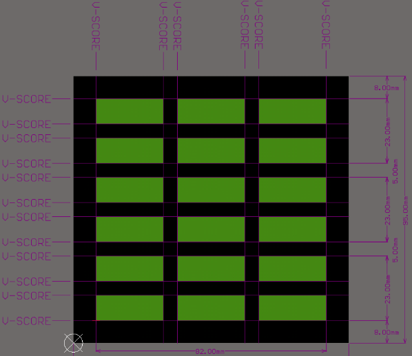
Drawing panel fabrication drawings is an integral step in the process of making PCBs. Fabrication drawings for individual PCBs only…
Circuit simulation software and PCB design software play complementary roles in the PCB design process, providing engineers with tools to…
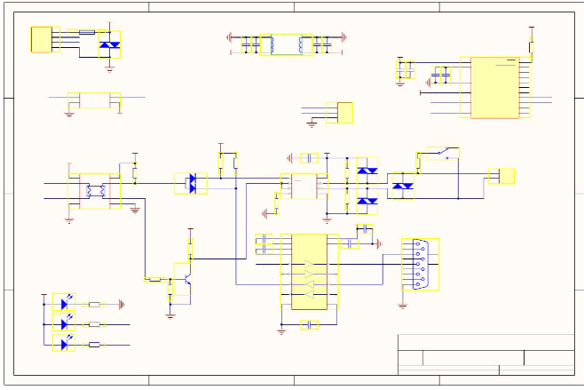
Schematic diagram production is the basis of PCB layout, so the schematic diagram restoration should be completed without errors. There…
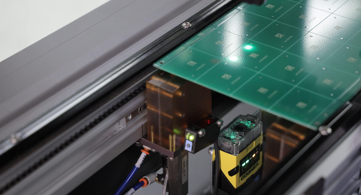
With the rapid increase in the demand for smart mobile equipment around the world, the demand for PCB depaneling machines…

1.Definition of gold finger (Gold Finger or Edge Connector) Insert one end of the PCB into the connector slot, use…
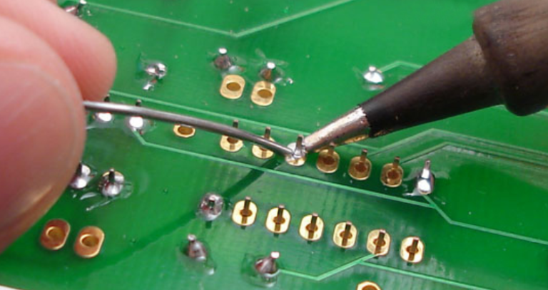
After the copper clad laminate is processed to produce printed circuit graphics, various vias, and assembly holes, various components are…
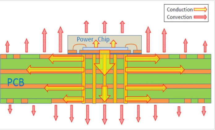
The measurement of PCB thermal resistance is a key step in evaluating the heat dissipation performance of printed circuit boards….
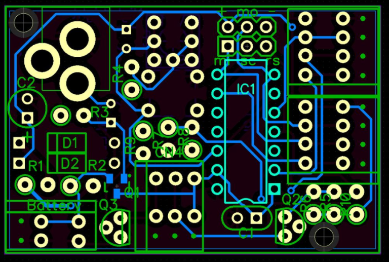
PCB circuit boards are important carriers of electronic components. In order to improve the yield rate and quality of electronic…
Introduction to PCB Film Types In printed circuit board (PCB) manufacturing, the terms “positive film” and “negative film” refer to…
Abstract This paper explores the critical relationship between printed circuit board (PCB) layout design for power supplies and electromagnetic compatibility…
In today’s era of rapid development of electronic technology, the design and welding technology of RF PCB circuit boards are…
Introduction In today’s increasingly visual world, camera systems have become ubiquitous across countless applications – from smartphones and security systems…
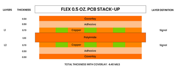
Introduction Printed Circuit Board (PCB) thickness stackup refers to the arrangement of copper layers and insulating materials that make up…
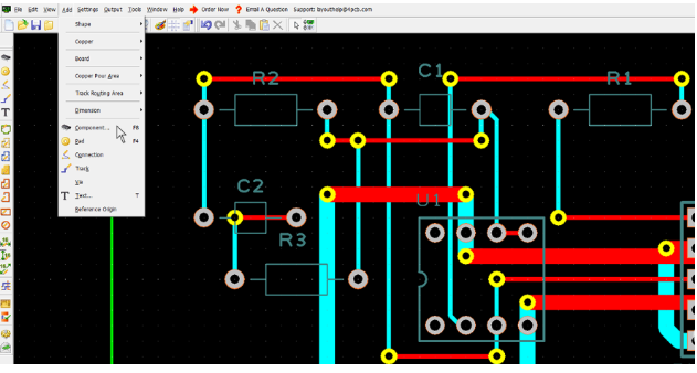
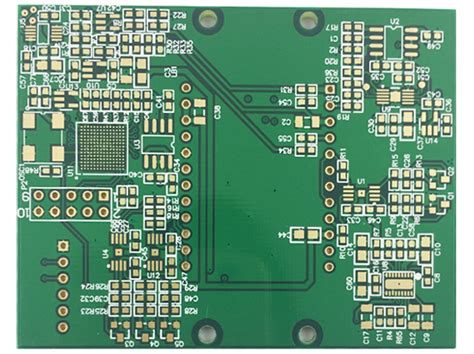
Introduction to PCB Layout Tools Printed Circuit Board (PCB) layout tools are specialized software applications that enable engineers and designers…
We use cookies to improve your experience on our site. By using our site, you consent to cookies.
Manage your cookie preferences below:
Essential cookies enable basic functions and are necessary for the proper function of the website.
Statistics cookies collect information anonymously. This information helps us understand how visitors use our website.
Google Analytics is a powerful tool that tracks and analyzes website traffic for informed marketing decisions.
Service URL: policies.google.com (opens in a new window)
SourceBuster is used by WooCommerce for order attribution based on user source.
You can find more information in our privacy policy and privacy policy.