Causes and Improvements of Deformation
When the circuit board is reflow soldered, it is easy to bend and warp the board. In severe cases, it may even cause empty soldering of components and erection of monuments. How to overcome it?
1.Hazards of PCB deformation
On the automated surface mount line, if the circuit board is not flat, it will cause inaccurate positioning, and the components cannot be inserted or mounted on the holes and surface mount pads of the board, and even damage the automatic insertion machine. The circuit board with components installed is bent after welding, and it is difficult to cut the component legs neatly. The board cannot be installed on the chassis or the socket inside the machine, so it is also very annoying for the assembly plant to encounter board warping. The current surface mount technology is developing towards high precision, high speed and intelligence, which puts forward higher flatness requirements for PCB boards as the home of various components.
In the IPC standard, it is specifically pointed out that the maximum deformation allowed for PCB boards with surface mount devices is 0.75%, and the maximum deformation allowed for PCB boards without surface mount devices is 1.5%. In fact, in order to meet the needs of high-precision and high-speed mounting, some electronic assembly manufacturers have stricter requirements on deformation. For example, our company has many customers who require the maximum deformation allowed to be 0.5%, and some even require 0.3%.
PCB boards are composed of copper foil, resin, glass cloth and other materials. The physical and chemical properties of each material are different. After being pressed together, thermal stress residue will inevitably occur, resulting in deformation. At the same time, during the processing of PCB, it will go through various processes such as high temperature, mechanical cutting, and wet treatment, which will also have an important impact on the deformation of the board. In short, the reasons that can cause PCB board deformation are complex and diverse. How to reduce or eliminate deformation caused by different material properties or processing has become one of the most complex problems faced by PCB manufacturers.
2.Analysis of the causes of deformation
The deformation of PCB boards needs to be studied from several aspects such as materials, structure, graphic distribution, and processing process. This article will analyze and explain the various reasons and improvement methods that may cause deformation.
The uneven copper surface area on the circuit board will worsen the board bending and warping.
Generally, a large area of copper foil is designed on the circuit board for grounding. Sometimes, the Vcc layer is also designed with a large area of copper foil. When these large areas of copper foil cannot be evenly distributed on the same circuit board, it will cause uneven heat absorption and heat dissipation speed. Of course, the circuit board will also expand and contract with heat. If the expansion and contraction cannot be simultaneous, it will cause different stresses and deformation. At this time, if the temperature of the board has reached the upper limit of the Tg value, the board will begin to soften and cause permanent deformation.
The connection points (vias) of each layer on the circuit board will limit the expansion and contraction of the board.
Most of the circuit boards today are multi-layer boards, and there are connection points (vias) like rivets between layers. The connection points are divided into through holes, blind holes and buried holes. The places with connection points will limit the expansion and contraction of the board, and will also indirectly cause board bending and warping.
The weight of the circuit board itself will cause the board to sag and deform.
Generally, the reflow furnace will use a chain to drive the circuit board forward in the reflow furnace, that is, the two sides of the board are used as fulcrums to support the entire board. If there are too heavy parts on the board, or the size of the board is too large, it will appear concave in the middle due to its own weight, causing the board to bend.
The depth of the V-Cut and the connecting strip will affect the deformation of the board.
Basically, the V-Cut is the culprit that destroys the board structure, because the V-Cut is to cut a groove on the original large sheet of board, so the V-Cut is prone to deformation. (Related reading: Circuit board edge removal—V-Cut board splitter)

2.1 Analysis of the impact of lamination materials, structures, and graphics on board deformation
PCB boards are laminated together with core boards, prepregs, and outer copper foils. The core boards and copper foils are deformed by heat during lamination, and the amount of deformation depends on the thermal expansion coefficient (CTE) of the two materials
The thermal expansion coefficient (CTE) of copper foil is about
While the Z-direction CTE of ordinary FR-4 substrates under Tg point is
;
Above TG point is (250~350)X10-6, and the X-direction CTE is generally similar to that of copper foil due to the presence of glass cloth.
/*Notes on TG point:
When the temperature of a high Tg printed board rises to a certain area, the substrate will change from “glass state” to “rubber state”, and the temperature at this time is called the glass transition temperature (Tg) of the board. In other words, Tg is the highest temperature (℃) at which the substrate maintains rigidity. That is to say, ordinary PCB substrate materials not only soften, deform, melt, etc. at high temperatures, but also show a sharp decline in mechanical and electrical properties.
Generally, the Tg of the board is above 130 degrees, the high Tg is generally greater than 170 degrees, and the medium Tg is about greater than 150 degrees.
PCB printed boards with Tg ≥ 170℃ are usually called high Tg printed boards.
With the increase of the Tg of the substrate, the heat resistance, moisture resistance, chemical resistance, stability resistance and other characteristics of the printed board will be improved and improved. The higher the TG value, the better the temperature resistance of the board. Especially in the lead-free process, high Tg is more widely used.
High Tg refers to high heat resistance. With the rapid development of the electronics industry, especially electronic products represented by computers, the development towards high functionality and high multi-layer requires higher heat resistance of PCB substrate materials as an important guarantee. The emergence and development of high-density mounting technologies represented by SMT and CMT have made PCBs increasingly dependent on the support of high heat resistance of substrates in terms of small apertures, fine circuits, and thinness.
Therefore, the difference between general FR-4 and high-Tg FR-4 is that in the hot state, especially when heated after moisture absorption, the mechanical strength, dimensional stability, adhesion, water absorption, thermal decomposition, thermal expansion and other conditions of the material are different. High-Tg products are obviously better than ordinary PCB substrate materials.
Among them, the expansion of the core board with the inner layer pattern is different due to the difference in pattern distribution and core board thickness or material properties. When the pattern distribution is different from the core board thickness or material properties, when the pattern distribution is relatively uniform and the material type is consistent, no deformation will occur. When the PCB board lamination structure is asymmetric or the pattern distribution is uneven, the CTE of different core boards will be greatly different, resulting in deformation during the lamination process. Its deformation mechanism can be explained by the following principles.
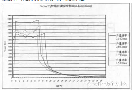
Figure 1 Dynamic viscosity curve of common prepreg
Suppose two core boards with large CTE difference are pressed together by prepreg, where CTE of core board A is 1.5×10⁻⁵/℃ and the length of core boards is 1000mm. The prepreg, which is used as bonding sheet in the pressing process, will bond two core boards together through three stages: softening, flowing and filling pattern, and curing.
Figure 1 is the dynamic viscosity curve of common FR-4 resin at different heating rates. Generally, the material starts to flow at about 90℃ and starts to cross-link and cure when it reaches above TG point. Before curing, the prepreg is in a free state. At this time, the core board and copper foil are in a free expansion state after being heated. The deformation can be obtained through their respective CTE and temperature change values.
Simulating the pressing condition, the temperature rises from 30℃ to 180℃, and the deformation of the two core boards is respectively
△LA=(180℃~30℃)x1.5×10-5m/℃X1000mm=2.25mm
△LB=(180℃~30℃)X2.5X10-5M/℃X1000mm=3.75mm
At this time, since the semi-curing is still in a free state, the two core boards are one long and one short, do not interfere with each other, and have not yet deformed.
As shown in Figure 2, during the lamination, the core board will be kept at high temperature for a period of time until the semi-cured board is completely cured. At this time, the resin becomes a solidified state and cannot flow freely, and the two core boards are combined together. When the temperature drops, if there is no interlayer resin constraint, the core board will return to its initial length and will not deform. However, in fact, the two core boards have been bonded by the cured resin at high temperature and cannot shrink freely during the cooling process. The A core board should shrink by 3.75mm. In fact, when the shrinkage is greater than 2.25mm, it will be hindered by the A core board. In order to achieve the force balance between the two core boards, the B core board cannot shrink to 3.75mm, and the A core board will shrink more than 2.25mm, so that the whole board will bend toward the B core board, as shown in Figure 2.

Figure 2 Schematic diagram of deformation during lamination of different CTE core boards
According to the above analysis, the lamination structure, material type and pattern distribution of the PCB board directly affect the CTE difference between different core boards and copper foils. The difference in expansion and contraction during the lamination process will be retained through the fixing process of the semi-cured sheet and eventually form the deformation of the PCB board.
2.2 Deformation caused during PCB processing
The causes of deformation during PCB processing are very complex and can be divided into two types of stress: thermal stress and mechanical stress. Thermal stress is mainly generated during the pressing process, while mechanical stress is mainly generated during the stacking, handling and baking of the panels. The following is a brief discussion in the order of the process.
Copper clad laminate materials: Copper clad laminates are all double-sided boards with symmetrical structures and no graphics. The CTE of copper foil and glass cloth is almost the same, so there is almost no deformation caused by different CTE during the pressing process. However, the size of the copper clad laminate press is large, and there is a temperature difference in different areas of the hot plate, which will lead to slight differences in the curing speed and degree of resin in different areas during the pressing process. At the same time, the dynamic viscosity at different heating rates is also quite different, so local stress caused by differences in the curing process will also be generated. Generally, this stress will maintain balance after pressing, but will gradually release and cause deformation in future processing.
Laminating: The PCB pressing process is the main process that produces thermal stress. The deformation caused by different materials or structures can be seen in the analysis in the previous section. Similar to the lamination of copper clad laminates, local stress caused by differences in the curing process will also be generated. Due to the thicker thickness, diverse pattern distribution, and more prepregs, the thermal stress of PCBs will be greater and more difficult to eliminate than copper clad laminates. The stress in the PCB is released in the subsequent drilling, contouring or baking processes, causing the board to deform.
Bake process of solder mask, characters, etc.: Since solder mask ink cannot be stacked on each other during curing, PCB boards are placed vertically in the rack for curing. The solder mask temperature is about 150℃, which just exceeds the Tg point of medium and low Tg materials. The resin above the Tg point is highly elastic, and the board is easily deformed under its own weight or strong wind in the oven.
Hot air solder leveling: When the ordinary board is leveled with hot air solder, the tin furnace temperature is 225℃~265℃, and the time is 3S-6S. The hot air temperature is 280℃~300℃. When the solder is leveled, the board enters the tin furnace from room temperature, and is washed with room temperature post-processing water within two minutes after leaving the furnace. The whole hot air solder leveling process is a sudden heating and cooling process. Due to the different materials and uneven structures of the circuit boards, thermal stress will inevitably occur during the hot and cold process, resulting in microscopic strain and overall deformation warping.
Storage: PCB boards are generally firmly inserted in the racks during the semi-finished stage. Improper adjustment of the rack tightness or stacking of boards during storage will cause mechanical deformation of the boards. Especially for thin boards below 2.0mm, the impact is more serious.
In addition to the above factors, there are many other factors that affect PCB deformation.
3.Improvement measures
How can we prevent the board from bending and warping when passing through the reflow furnace?
(1)Reduce the impact of temperature on board stress
Since “temperature” is the main cause of board stress, as long as the temperature of the reflow furnace is reduced or the speed of heating and cooling of the board in the reflow furnace is slowed down, the occurrence of board bending and warping can be greatly reduced. However, there may be other side effects.
(2)Use high Tg boards
Tg is the glass transition temperature, which is the temperature at which the material changes from glass to rubber. The lower the Tg value of the material, the faster the board will soften after entering the reflow furnace, and the longer it will take to become soft and rubbery. The deformation of the board will of course be more serious. Using a board with a higher Tg can increase its ability to withstand stress deformation, but the price of the material is relatively high.
(3)Increase the thickness of the circuit board
In order to achieve the purpose of being thinner and lighter, the thickness of many electronic products has been reduced to 1.0mm, 0.8mm, or even 0.6mm. It is really difficult to keep the board from deforming after passing through the reflow furnace. It is recommended that if there is no requirement for thinness, the board should be 1.6mm thick, which can greatly reduce the risk of bending and deformation.
(4)Reduce the size of the circuit board and the number of panels
Since most reflow ovens use chains to drive the circuit board forward, the larger the size of the circuit board, the more likely it is to be dented and deformed in the reflow oven due to its own weight. Therefore, try to put the long side of the circuit board as the board side and place it on the chain of the reflow oven to reduce the dent deformation caused by the weight of the circuit board itself. The reason for reducing the number of panels is also based on this. That is to say, when passing through the oven, try to use the narrow side perpendicular to the direction of passing through the oven to achieve the lowest dent deformation.
(5)Use a reflow tray fixture
If the above methods are difficult to achieve, the last step is to use a reflow tray (reflow carrier/template) to reduce the deformation. The reason why the reflow tray can reduce the bending and warping of the board is that no matter it is thermal expansion or cold contraction, it is hoped that the tray can fix the circuit board until the temperature of the circuit board is lower than the Tg value and begins to harden again, and the original size can be maintained.
If a single-layer tray still cannot reduce the deformation of the circuit board, it is necessary to add another layer of cover and clamp the circuit board with the upper and lower trays. This can greatly reduce the problem of deformation of the circuit board when passing through the reflow oven. However, the furnace pallet is quite expensive, and it takes manpower to place and recycle the pallet.
(6)Use real connection and stamp hole instead of V-Cut to separate the boards
Since V-Cut will destroy the structural strength of the boards between the circuit boards, try not to use V-Cut to separate the boards, or reduce the depth of V-Cut.

Real connection: use a knife-type board separation machine

Stamp hole
Optimization in PCB production engineering:
The influence of different materials on board deformation
The deformation defect rate of boards of different materials exceeding the standard is counted, and the results are shown in Table 1.

As can be seen from the table, the deformation defect rate of low Tg materials is higher than that of high Tg materials. The high Tg materials listed in the above table are all filler-shaped materials, and their CTE is lower than that of low TgMaterials, and in the processing after lamination, the baking temperature is up to 150℃, which will definitely have a greater impact on low Tg materials than medium and high Tg materials.
Engineering design research
Engineering design should try to avoid asymmetric structures, asymmetric materials, and asymmetric graphics to reduce deformation. At the same time, it was found in the research process that the core board direct lamination structure is more likely to deform than the copper foil lamination structure. Table 2 shows the test results of the two structural panels.

From Table 2, it can be seen that the defect rate of the two structures with unqualified deformation is significantly different. It can be understood that the core board lamination structure is composed of three core boards, and the expansion and contraction and stress changes between different core boards are more complicated and more difficult to eliminate.
In engineering design, the form of the panel frame also has a great influence on deformation. Generally, PCB factories will have continuous large copper skin frames and discontinuous copper points or copper block frames, which are also different.
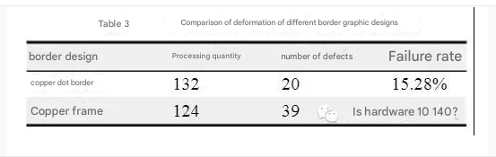
Table 3 shows the comparative test results of the two frame design panels. The reason why the deformation performance of the two frame forms is different is that the continuous copper frame has high strength and is relatively rigid during the pressing and panel processing, which makes it difficult to release the residual stress in the board. The release is concentrated after the shape processing, resulting in more serious deformation. The non-continuous copper point frame gradually releases stress during the pressing and subsequent processing, and the deformation of the single board is small after the shape.
The above are some possible influencing factors involved in engineering design. If they can be flexibly used in the design. It can reduce the deformation caused by the design.
3.3 Pressing research
The influence of pressing on deformation is crucial. The generation of stress can be effectively reduced by reasonable parameter setting, press selection and stacking method. For general structural symmetrical panels, it is generally necessary to pay attention to symmetrical stacking during pressing, and symmetrical placement of auxiliary tools such as tool plates and buffer materials. At the same time, choosing a hot and cold integrated press for pressing can also significantly help reduce thermal stress. The reason is that the hot and cold split press transfers the board to the cold press at high temperature (above GT temperature). The material loses pressure above the Tg point and cools quickly, which will cause the thermal stress to be quickly released and deformed. The hot and cold integrated press can achieve cooling at the end of hot pressing to avoid the board losing pressure at high temperature.
At the same time, for the special needs of customers, there will inevitably be some boards with asymmetric materials or structures. At this time, the deformation caused by different CTEs analyzed in the previous article will be very obvious. For this problem, we can try to use an asymmetric stacking method to solve it. The principle is to use the asymmetric placement of buffer materials to achieve different heating speeds on both sides of the PCB board, thereby affecting the expansion and contraction of different CTE core cypresses in the heating and cooling stages to solve the problem of inconsistent deformation. Table 4 is the test results on a certain structural asymmetric board of our company.
Through the asymmetric stacking method, adding a post-curing process after pressing, and leveling before shipment, this board finally meets the customer’s 2.0mm requirement.

3.4 Other production processes
In the PCB production process, in addition to lamination, there are several high-temperature processing processes such as solder mask, characterization and hot air leveling. The highest temperature of the baking plate after solder mask and characterization is 150℃. As mentioned in the previous article, this temperature is above the Tg point of ordinary Tg materials. At this time, the material is in a highly elastic state and is easily deformed under external force. Therefore, it is necessary to avoid stacking the plates during baking to prevent the lower plate from being bent. At the same time, the direction of the plate should be parallel to the blowing direction during baking. During hot air leveling, it is necessary to ensure that the plate is flat and cooled for more than 30 seconds after leaving the tin furnace to avoid sudden cooling and deformation caused by cold water washing after post-treatment at high temperature.
In addition to the production process, the storage of PCB boards at each station also has a certain impact on deformation. In some manufacturers, due to the large number of waiting for production and small space, multiple racks of boards will be stacked together for storage, which will also cause the board to be deformed by external force. Since the PCB board also has a certain plasticity, these deformations will not be 100% restored in the subsequent leveling process.
3.5 Leveling before shipment
Most PCB manufacturers have a leveling process before shipment. This is because the board deformation caused by heat or mechanical force will inevitably occur during the processing process. Mechanical leveling or hot baking leveling before shipment can effectively improve it. Affected by the heat resistance of solder resist and surface coating layer, the general baking temperature is below 140℃~150℃, just exceeding the Tg temperature of ordinary materials. This is very beneficial to the leveling of ordinary boards, but the leveling effect on high Tg materials is not so obvious. Therefore, the baking temperature can be appropriately increased on individual high Tg boards with severe warping, but the quality of ink and coating layer should be paid attention to. At the same time, the practice of pressing weight and increasing the cooling time with the furnace during baking also has a certain improvement effect on deformation. Table 5 shows the test results of the leveling effect of different pressing weights and furnace cooling time on the board. It can be seen that increasing the pressing weight and extending the furnace cooling time have a significant effect on the leveling of deformation.


