Causes of PCB delamination and blistering How to prevent PCB delamination?
Today is mainly about: PCB delamination, causes and solutions for PCB delamination and blistering, PCB delamination repair
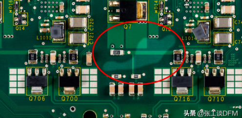
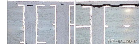
I believe that engineers will encounter PCB delamination when making boards. The following picture is what an engineer recently reported after the board was made. Look at the arrows in the picture, it is obviously delaminated. This article will talk about delamination.
I.PCB delamination
PCB delamination is a type of damage that may occur in PCBs, which will cause the substrate layers to separate from each other.
Blistering: A form of delamination that manifests as local expansion and separation between any layers of the laminated substrate, or between the substrate and the conductive film or protective layer
Delamination: Separation between layers of the substrate in the printed board, between the substrate and the conductive foil or other.
If it is external, it is usually easy to see that there will be small bubbles or gaps. As shown in the following two pictures:
PCB delamination
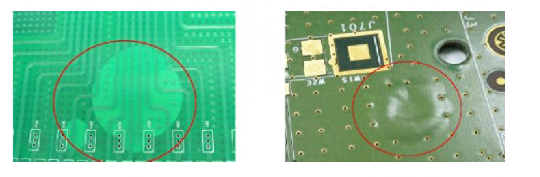
PCB delamination and blistering
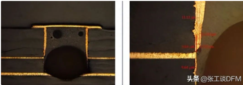
In addition to PCB delamination on the outside, it also occurs on the inside. When delamination occurs on the internal layer, it may cause failure. If the PCB delamination is not thoroughly checked, it is difficult to find out the cause of the failure.
The following is a PCB internal short defect, which occurs in the process of transferring from the internal layer to the multi-layer lamination.
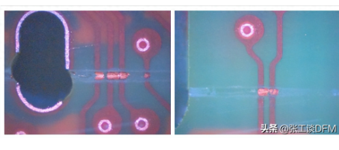
PCB internal short defect
II.Causes of PCB delamination and blistering
Here is a picture from Teacher Xu Lin, which comes from the failure case summary in the factory, and also collects the on-site experience of the PCB board factory and the analysis data of peers in the industry.
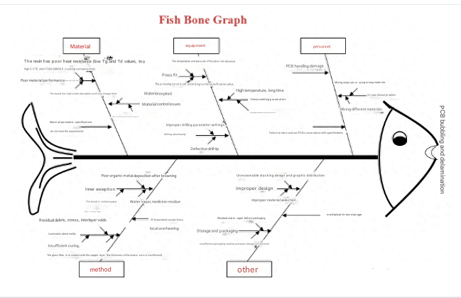
Causes of PCB bubbles
The following is also a picture from Teacher Xu Lin, which comes from the summary of failed product data in the assembly plant and the PCB board factory, and has a certain reference value for PCB delamination and blistering.
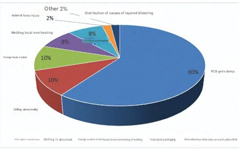
Analysis of causes of PCB delamination bubbles
The above is a summary, and the following is a more specific analysis, of course, it is just a reference.
1.PCB dampness
The most common cause of PCB delamination is excessive humidity. The presence of humidity can cause condensation and frost, which can cause PCB thermal shock damage. This type of damage can cause delamination over time or immediately after a surge.
Temperature
Moisture accumulation in the PCB substrate is one of the most typical causes of delamination. Moisture causes CAF (conductive anodic filaments), where water enters an electrochemical reaction that creates tiny filaments. These filaments can bridge conductors, causing short circuits.
When the temperature rises in later processing steps, this moisture turns into vapor. For example, the reflow soldering process occurs at temperatures above 200°C. Such heat levels are well above the boiling temperature of water and convert moisture into vapor.
The pressure from this vapor interferes with curing and lamination, tearing some parts apart. These separated parts or bubbles may appear immediately or later during subsequent heat treatment steps or large thermal excursions when the printed circuit board is in use.
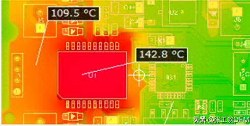
2.Thermal stress
PCBs are prone to thermal stress because they are manufactured using multiple layers of copper and other materials that are bonded together with heat-curing adhesives.
As temperature changes, this adhesive fails at holding the board together. The board may still work fine when it is cold, but as it warms up, it will start to separate.
PCB delamination diagram
3.Failure of solder mask
PCBs are usually made of double-sided FR-4 substrate material. Both sides of the substrate have a thin layer of epoxy resin. A layer of copper is applied to one side and then covered with a protective coating to prevent oxidation or corrosion during use.
The protective coating on one side of the circuit board is called solder mask because its purpose is to prevent solder from sticking to copper areas that should not be soldered. When the solder mask is exposed due to delamination, it may provide entry points for water or other contaminants that can cause corrosion and ultimately cause failure over time.
4.Poor manufacturing process
1) Substrate process treatment problems
For some relatively thin substrates, the rigidity is poor, and it is not suitable to use a brushing machine to brush the board, which will result in the inability to effectively remove the protective layer to prevent the copper foil on the board from oxidizing during the production and processing of the substrate. It is easy to cause blistering, and there will also be problems such as blackening, browning, and uneven color.
The following figure shows the stratified blistering on the copper foil.
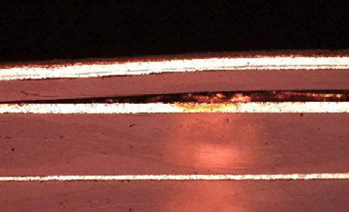
Stratified blistering on the copper foil
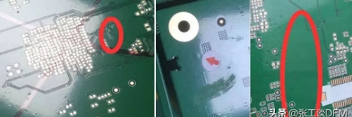
2) The surface of the board is contaminated with oil or other liquids and dust during machining (drilling, lamination, milling, etc.) and the surface treatment is poor
3) Poor copper brushing
The pressure of the grinding plate before copper deposition is too high, causing the hole to deform, brush out the fillet of the hole copper foil, and even leak the base material at the hole, which will cause blistering at the hole during copper deposition, electroplating, tin spraying, welding, etc.
4) Washing problem
Because the copper plating treatment needs to be treated with a large amount of chemical solutions, there are many kinds of acid, alkali, non-polar organic and other chemical solvents. If the board surface is not washed cleanly, it will not only cause cross contamination, but also cause poor local treatment or poor treatment effect and uneven defects on the board surface.
5) Micro-etching in the pre-treatment of copper plating and the pre-treatment of graphic electroplating
Excessive micro-etching will cause the hole to leak the substrate and cause blistering around the hole; insufficient micro-etching will also cause insufficient bonding force and cause blistering.
6) Poor copper rework
Some reworked boards after copper plating or graphic transfer have poor deplating during the rework process. Incorrect rework methods or improper micro-etching time control during the rework process or other reasons will cause blistering on the board surface.
7) Oxidation of the board surface during the production process
If the copper plating board oxidizes in the air, it may not only cause no copper in the hole and rough board surface, but also cause blistering on the board surface. If the copper plating board is stored in the acid solution for too long, the board surface will also oxidize, and this oxide film is difficult to remove.
5.Poor quality materials
When your PCB is of low quality, there is a higher chance of failure and starting to separate.
6.Wrong type of FR-4 Tg material
It is very important to use the right type of FR-4Tg material when manufacturing PCBs. FR-4Tg material is an epoxy resin used to manufacture PCBs.
Choosing to use the wrong type of FR-4Tg material may cause the PCB to delaminate and fall apart prematurely. This may cause problems with reliability and service life, resulting in higher manufacturing costs for you.
III. How to prevent PCB delamination?
1.Manufacturing process
For the reflow soldering curve, it is recommended that the temperature curve be set to meet the specifications and the solder joint quality meets the quality standards in the early stage, and the soldering time and temperature should be shortened as much as possible to reduce the heating of the board.
2.Material selection
The selection of the substrate should try to use qualified materials, and the quality of the PP material of the multilayer board is also a key parameter.
3.Lamination process control in place
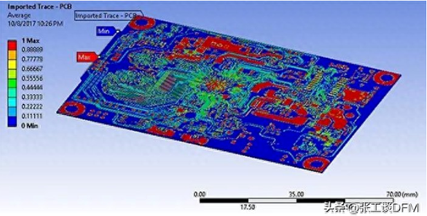
The lamination process control is in place, especially for multilayer boards with thick inner copper foil, more attention should be paid. Under thermal shock, the inner layer of the multilayer board delaminated, resulting in the scrapping of the entire batch. The following is a picture of poor lamination process.
Poor lamination process
Poor lamination process
4.Copper deposition quality
The denser the copper layer on the inner wall of the hole, the thicker the copper layer, the stronger the thermal shock of the PCB circuit board. Both PCB circuit boards have high reliability and low manufacturing cost, and each step of the electroplating process control requires refined control.
5.Incoming materials for assembled PCBs
Incoming materials of components are very important, especially for component suppliers during storage. If they are not stored under suitable conditions, the components are likely to fail. If they are not found during assembly, it is easy to cause the entire PCBA to fail when the assembly is completed.
6.Dry storage
Delamination occurs when the PCB is exposed to moisture or humidity. If the PCB is to be stored for a long time, it must be kept dry. The best way is to store the PCB in a closed container to prevent moisture from penetrating.
Causes of PCB delamination It is necessary to fundamentally prevent the delamination of PCB circuit boards, which is something that every excellent PCB manufacturer should learn.
IV. PCB delamination test
There are several types of tests that can be used to measure delamination. The most common ones are scanning acoustic microscopy and thermomechanical analysis, including bubbles in the coating, delamination, fractures or other anomalies.
1.Scanning acoustic microscopy
Scanning acoustic microscopy is a non-destructive testing method that uses ultrasound to measure the thickness of the material. It is particularly useful for detecting delamination.
That is, when the two bonded surfaces are separated, the test uses a laser to scan the surface of the material. The laser can create a topographic map of the sample, which can determine whether there are any cracks or other defects. It is also one of the most commonly used methods for detecting delamination of composite materials.
Scanning Acoustic Microscope
2.Thermomechanical Analysis
This test measures the energy required to break a sample. The thermomechanical analyzer applies pressure to the sample and then measures the force required to break the sample.
If delamination is not present, this test should not show any change in breaking force or energy. It is used to determine the mechanical properties of a material, including its elasticity and strength. It is often used to measure the delamination of a material and can be used to determine the quality of adhesives, coatings, and other products.
3.Stress Test Parameters – Floating Solder Test
Stress Test Parameters for PCB Delamination: is an accelerated life test that simulates the effects of solder joints being subjected to thermal cycles. The solder joints are subjected to six times the number of thermal cycles in normal applications. The test is performed at 288°C, which is higher than the typical operating temperature of most electronic components.
4.Reflow Simulation N Passes
A common test method is to simulate a high-temperature reflow process by heating and cooling the PCB multiple times. Each time you heat and cool the PCB in this test, it is called an “N pass”. The number of passes where you don’t see delamination is the maximum N number of passes you are allowed.
5.Interconnect Stress Test
Without proper testing, common modes will roam freely throughout the board, often destroying the integrity of traces and pads or causing near failures. By performing an interconnect stress test, engineers can pull out the common mode, thereby reducing these problems.
This simple test can be performed to save millions of dollars in production costs by identifying whether a printed circuit board is at risk before manufacturing. A test that simulates the thermal cycling conditions that a component will experience during its service life. This test is performed by applying a static force (6X@230°C) to the PCB. The static force is applied for 10 seconds and then released for 30 seconds. The cycle is repeated for one minute. The test duration is kept at minutes to ensure that all material properties are tested under the same conditions.
IIV.Solutions to PCB delamination and blistering
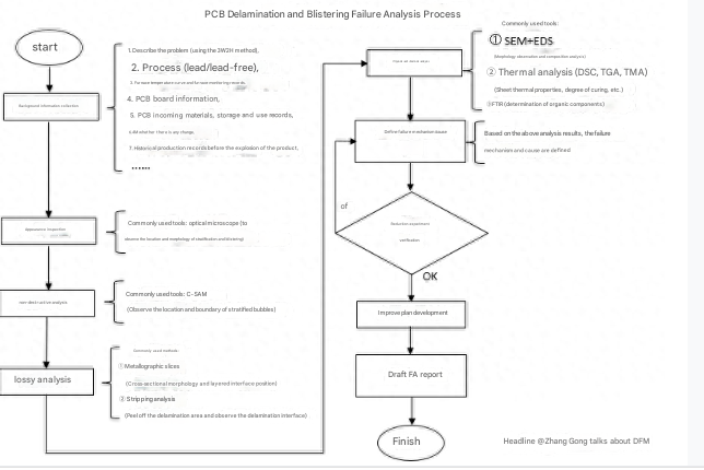
The following is the PCB delamination and blistering failure analysis process, which comes from Teacher Xu Lin’s figure.
The following is how to repair PCB delamination? (The following method is for reference only. It is recommended to let the PCB manufacturer handle it. Professional things should be left to professionals)
1.Prepare materials
Abrasives, ball mills, cutting tools
Circuit bonding epoxy
Microscope
Microdrill system
Stirring pick
Syringe
Oven
Wet wipes
2.Steps
Use wet wipes to clean the surface of the blister
Drill at least two holes in the delaminated blister using a ball mill and a micro drill. The holes should be opposite each other and around the perimeter of the blister. In addition, they should be free of any components or circuits. Brush off loose material after drilling.
Note: Do not drill too deep to expose internal planes or circuits. Remember that grinding operations can generate static charges.
Bake the circuit board in an oven to eliminate any moisture. Do not let it cool before injecting epoxy, as moisture may condense and become trapped inside again.
Note: Some electronic components are sensitive to high temperatures. Don’t get the temperature too high.
Pour the epoxy into a cartridge and inject it into one of the drilled holes. The heat from the PCB should help disperse the epoxy, drawing it into the void area to fill the space.
If the blister is not filled, apply gentle pressure to the board. Start with the filling hole and slowly work your way into the vent hole. Alternatively, you can vacuum the vent hole to pull the epoxy out and fill the void.
Cure the epoxy at room temperature for 24 hours or at 74°C (165°F) for one hour.
Use a scraper or knife to scrape off any excess epoxy. Apply a thin coat if necessary to seal the scrapped area.
3.Inspection
After drying, visually inspect the color and texture. Also, electrically test the conductors around the repair area to see if everything is OK.
Although there are ways to fix PCB delamination blistering, it’s best to nip this in the bud and prevent it in advance, which can save time and cost.