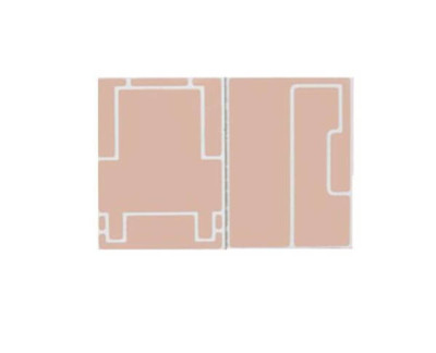
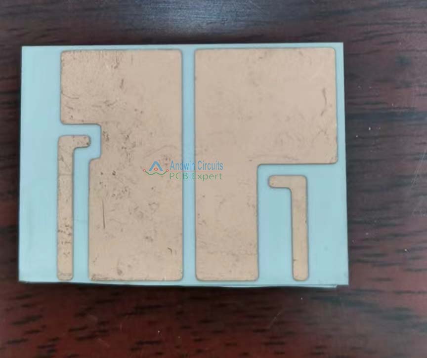
Ceramic base pcb
Advantages Of Using Ceramic Base PCB In High-Frequency Applications
Ceramic base printed circuit boards (PCBs) have emerged as a pivotal technology in the realm of high-frequency applications, offering a multitude of advantages that make them indispensable in various advanced electronic systems.
One of the primary benefits of ceramic base PCBs is their exceptional thermal conductivity.
Unlike traditional materials such as FR4, ceramics like aluminum oxide (Al2O3) and aluminum nitride (AlN) can efficiently dissipate heat, ensuring that electronic components remain within their optimal operating temperatures. This characteristic is particularly crucial in high-frequency applications where excessive heat can lead to performance degradation and potential failure of the electronic components.
In addition to superior thermal management, ceramic base PCBs exhibit remarkable electrical insulation properties.
The high dielectric strength of ceramic materials ensures minimal electrical interference, which is essential for maintaining signal integrity in high-frequency circuits. This attribute is further complemented by the low dielectric constant and low loss tangent of ceramics, which contribute to reduced signal loss and enhanced performance of high-frequency signals. Consequently, devices that rely on precise and stable signal transmission, such as RF modules and microwave circuits, greatly benefit from the use of ceramic base PCBs.
Moreover, the mechanical robustness of ceramic base PCBs cannot be overstated.
Ceramics are inherently resistant to mechanical stress, vibration, and environmental factors such as moisture and chemicals. This durability ensures that the PCBs can withstand harsh operating conditions, making them ideal for aerospace, military, and automotive applications where reliability is paramount. The ability to maintain structural integrity under extreme conditions not only extends the lifespan of the electronic devices but also reduces the need for frequent maintenance and replacements.
Another significant advantage of ceramic base PCBs is their compatibility with advanced manufacturing techniques.
The precision and versatility of ceramic materials allow for the integration of fine-pitch components and complex circuit designs. This capability is particularly beneficial in the miniaturization of electronic devices, where space constraints demand highly compact and efficient circuit layouts. Furthermore, ceramic base PCBs can be fabricated using various methods such as thick-film, thin-film, and low-temperature co-fired ceramic (LTCC) technologies, providing designers with a wide range of options to meet specific application requirements.
The environmental stability of ceramic base PCBs also plays a crucial role in their adoption for high-frequency applications.
Ceramics are inherently stable over a wide range of temperatures and frequencies, ensuring consistent performance even under fluctuating environmental conditions. This stability is essential for applications that require long-term reliability and precision, such as medical devices and telecommunications equipment. Additionally, the inert nature of ceramics makes them resistant to oxidation and corrosion, further enhancing their longevity and reliability.
In conclusion, the advantages of using ceramic base PCBs in high-frequency applications are manifold. Their superior thermal conductivity, excellent electrical insulation properties, mechanical robustness, compatibility with advanced manufacturing techniques, and environmental stability collectively make them an ideal choice for a wide range of advanced electronic systems. As the demand for high-performance and reliable electronic devices continues to grow, the adoption of ceramic base PCBs is likely to expand, driving further innovations and advancements in the field of high-frequency electronics.
Thermal Management Solutions With Ceramic Base PCB
In the realm of modern electronics, thermal management has emerged as a critical factor influencing the performance, reliability, and longevity of devices. As electronic components become increasingly powerful and compact, the need for efficient heat dissipation solutions has never been more pressing.
One innovative approach that has gained significant traction is the use of ceramic base printed circuit boards (PCBs).
These advanced substrates offer a myriad of benefits, particularly in the context of thermal management, making them an indispensable asset in high-performance electronic applications.
Ceramic base PCBs are distinguished by their exceptional thermal conductivity, which is a direct consequence of the inherent properties of ceramic materials.
Unlike traditional FR4 substrates, which are composed of woven glass fabric and epoxy resin, ceramic materials such as aluminum oxide (Al2O3), aluminum nitride (AlN), and beryllium oxide (BeO) exhibit superior thermal conductivity.
This characteristic enables ceramic base PCBs to efficiently dissipate heat away from critical components, thereby mitigating the risk of thermal-induced failures and enhancing overall system reliability.
Moreover, the thermal expansion coefficient of ceramic materials closely matches that of silicon, the primary material used in semiconductor devices. This compatibility minimizes the mechanical stress that arises from thermal cycling, which is a common occurrence in electronic devices subjected to varying operational temperatures. Consequently, ceramic base PCBs contribute to the structural integrity and durability of electronic assemblies, particularly in applications where thermal stability is paramount.
In addition to their thermal management capabilities, ceramic base PCBs offer excellent electrical insulation properties.
This dual functionality is particularly advantageous in high-voltage and high-frequency applications, where maintaining electrical isolation while ensuring efficient heat dissipation is crucial. The robust dielectric strength of ceramic materials ensures that electronic components remain electrically isolated, thereby preventing short circuits and enhancing the safety and reliability of the overall system.
Furthermore, ceramic base PCBs are inherently resistant to environmental factors such as moisture, chemicals, and radiation.
This resilience makes them suitable for use in harsh operating conditions, including aerospace, automotive, and industrial applications. The ability to withstand extreme environments without compromising performance underscores the versatility and robustness of ceramic base PCBs, positioning them as a preferred choice for mission-critical applications.
The manufacturing process of ceramic base PCBs also contributes to their superior performance characteristics.
Advanced fabrication techniques, such as thick-film and thin-film deposition, allow for precise control over the thickness and composition of conductive and insulating layers. This precision ensures optimal thermal and electrical performance, tailored to the specific requirements of each application. Additionally, the use of laser drilling and metallization processes enables the creation of intricate circuit patterns and interconnections, further enhancing the functionality and complexity of ceramic base PCBs.
While the benefits of ceramic base PCBs are undeniable, it is important to acknowledge the associated challenges.
The cost of ceramic materials and the complexity of the manufacturing process can result in higher production costs compared to traditional FR4 substrates. However, the long-term advantages in terms of thermal management, reliability, and performance often justify the initial investment, particularly in high-stakes applications where failure is not an option.
In conclusion, ceramic base PCBs represent a significant advancement in thermal management solutions for modern electronics. Their exceptional thermal conductivity, electrical insulation properties, and environmental resilience make them an ideal choice for high-performance applications. As the demand for more powerful and compact electronic devices continues to grow, the adoption of ceramic base PCBs is poised to play a pivotal role in ensuring the reliability and longevity of next-generation technologies.
Manufacturing Process Of Ceramic Base PCB
The manufacturing process of ceramic base PCBs, or printed circuit boards, is a sophisticated and intricate procedure that demands precision and expertise. Ceramic base PCBs are highly valued in various industries due to their superior thermal conductivity, mechanical strength, and electrical insulation properties.
These attributes make them ideal for applications in high-power and high-frequency devices. To understand the manufacturing process, it is essential to delve into the various stages involved, from material selection to the final inspection.
Initially, the process begins with the selection of the ceramic substrate.
Common materials used include alumina (Al2O3), aluminum nitride (AlN), and beryllium oxide (BeO). Each of these materials offers distinct advantages, such as high thermal conductivity and excellent electrical insulation. The choice of substrate material is crucial as it directly impacts the performance and reliability of the final product. Once the appropriate material is selected, it is cut into the desired shape and size using precision cutting tools.
Following the substrate preparation, the next step involves the application of a conductive layer.
This is typically achieved through a process known as screen printing.
A conductive paste, often composed of metals like silver, gold, or copper, is applied to the ceramic substrate using a stencil or screen. The paste is then dried and cured at high temperatures to ensure strong adhesion to the substrate. This step is critical as it forms the basis for the electrical pathways on the PCB.
Subsequently, the circuit pattern is created through a process called photolithography.
A photosensitive material, known as a photoresist, is applied over the conductive layer. The desired circuit pattern is then transferred onto the photoresist using ultraviolet (UV) light. Areas exposed to the UV light harden, while unexposed areas remain soft and can be washed away using a developer solution. This leaves behind a precise circuit pattern on the conductive layer.
To enhance the durability and performance of the PCB, additional layers of conductive material may be added through a process called electroplating. This involves immersing the PCB in a solution containing metal ions and applying an electric current. The metal ions are deposited onto the exposed conductive areas, forming a thicker and more robust conductive layer. This step is particularly important for applications requiring high current-carrying capacity.
Once the circuit pattern is established, the next phase involves the application of a protective layer.
This is typically achieved through a process known as solder mask application. A layer of solder mask material is applied over the entire surface of the PCB, except for the areas where components will be soldered. The solder mask not only protects the conductive traces from oxidation and corrosion but also prevents solder bridges during the assembly process.
The final stages of the manufacturing process involve drilling and routing.
Precision drilling machines are used to create holes for component leads and vias, which are essential for establishing electrical connections between different layers of the PCB. Routing, on the other hand, involves cutting the PCB into its final shape and size using specialized cutting tools.
After all these steps are completed, the PCB undergoes rigorous testing and inspection to ensure it meets the required specifications and quality standards. This includes electrical testing to verify the integrity of the circuit connections and visual inspection to check for any defects or irregularities.
In conclusion, the manufacturing process of ceramic base PCBs is a meticulous and multi-faceted procedure that requires careful attention to detail at every stage. From material selection to final inspection, each step plays a crucial role in ensuring the performance and reliability of the final product. As technology continues to advance, the demand for high-performance ceramic base PCBs is expected to grow, further underscoring the importance of mastering this complex manufacturing process.
Comparing Ceramic Base PCB To Traditional FR4 PCB
When it comes to printed circuit boards (PCBs), the choice of material can significantly impact the performance, reliability, and cost of the final product.
Two of the most commonly used materials in PCB manufacturing are ceramic and FR4. While both have their own set of advantages and disadvantages, understanding the differences between ceramic base PCBs and traditional FR4 PCBs can help engineers and designers make more informed decisions.
Ceramic base PCBs are known for their excellent thermal conductivity and high-temperature resistance. These properties make them ideal for applications that require efficient heat dissipation, such as power electronics, LED lighting, and high-frequency circuits.
The ceramic material, typically aluminum oxide (Al2O3) or aluminum nitride (AlN), provides a stable and robust platform that can withstand extreme temperatures and harsh environmental conditions. This is particularly beneficial in industries like aerospace, automotive, and military, where reliability and durability are paramount.
In contrast, traditional FR4 PCBs are made from a composite material consisting of woven fiberglass cloth with an epoxy resin binder that is flame resistant. FR4 stands for “Flame Retardant 4,” indicating its excellent fire-resistant properties. FR4 PCBs are widely used in consumer electronics, telecommunications, and general industrial applications due to their cost-effectiveness and versatility. They offer a good balance of mechanical strength, electrical insulation, and thermal stability, making them suitable for a wide range of applications.
One of the primary differences between ceramic base PCBs and FR4 PCBs is their thermal performance.
Ceramic materials have a much higher thermal conductivity compared to FR4, which means they can dissipate heat more efficiently. This is crucial in high-power applications where excessive heat can lead to component failure or reduced performance. For instance, in LED lighting systems, ceramic base PCBs can help maintain optimal operating temperatures, thereby extending the lifespan of the LEDs and improving overall efficiency.
Another significant difference lies in the dielectric properties of the materials.
Ceramic base PCBs exhibit lower dielectric losses and higher dielectric strength compared to FR4. This makes them suitable for high-frequency applications where signal integrity is critical. In RF and microwave circuits, the superior dielectric properties of ceramic materials can result in better performance and reduced signal loss, which is essential for maintaining the integrity of high-speed data transmission.
However, it is important to consider the cost implications when choosing between ceramic base PCBs and FR4 PCBs. Ceramic materials are generally more expensive than FR4, both in terms of raw material costs and manufacturing processes. The higher cost can be justified in applications where the performance benefits outweigh the additional expense. For example, in high-reliability sectors like aerospace and military, the enhanced thermal and dielectric properties of ceramic base PCBs can provide a significant advantage.
In summary, the choice between ceramic base PCBs and traditional FR4 PCBs depends on the specific requirements of the application. Ceramic base PCBs offer superior thermal conductivity, high-temperature resistance, and excellent dielectric properties, making them ideal for high-power and high-frequency applications. On the other hand, FR4 PCBs provide a cost-effective and versatile solution for a wide range of general-purpose applications. By carefully evaluating the performance needs and budget constraints, engineers and designers can select the most appropriate material to ensure the success of their projects.


