Ceramic Hybrid PCB: Revolutionizing Modern Electronics
Introduction to Ceramic Hybrid PCBs
In the rapidly evolving world of electronics, Ceramic Hybrid Printed Circuit Boards (PCBs) have emerged as a groundbreaking solution for high-performance applications. These advanced circuit boards combine the superior properties of ceramic materials with traditional PCB technologies to create substrates that outperform conventional FR4 boards in demanding environments.
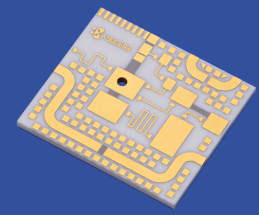
Ceramic hybrid PCBs represent a fusion of ceramic substrates (typically alumina, aluminum nitride, or beryllium oxide) with organic PCB materials, offering a unique combination of thermal conductivity, electrical insulation, and mechanical stability. This hybrid approach addresses many limitations of traditional PCBs while maintaining manufacturability and cost-effectiveness for specialized applications.
Materials and Composition
Ceramic Substrates
The foundation of ceramic hybrid PCBs lies in their ceramic components, which typically include:
- Alumina (Al₂O₃): The most common ceramic substrate material, offering good thermal conductivity (24-28 W/mK), excellent electrical insulation, and mechanical strength. Available in various purity levels (96%, 99.6%).
- Aluminum Nitride (AlN): Provides exceptional thermal conductivity (140-180 W/mK) with excellent electrical insulation, making it ideal for high-power applications.
- Beryllium Oxide (BeO): Offers the highest thermal conductivity among ceramics (250-300 W/mK) but presents health hazards during machining.
- Silicon Carbide (SiC): Used in extreme environments due to its thermal and chemical stability.
Hybrid Construction
The hybrid nature of these PCBs combines ceramic substrates with:
- Organic dielectric layers (polyimide, epoxy)
- Copper conductive layers (thick-film or thin-film)
- Specialized bonding materials
- Thermal interface materials
This combination allows for multilayer constructions that leverage the benefits of both ceramic and organic materials while mitigating their individual limitations.

Manufacturing Process
The production of ceramic hybrid PCBs involves specialized techniques that differ from conventional PCB manufacturing:
- Ceramic Substrate Preparation: Raw ceramic powders are formed into sheets through tape casting or pressing, then fired at high temperatures (1500-1800°C) to achieve dense substrates.
- Surface Finishing: Ceramic surfaces are polished and cleaned to ensure proper adhesion of subsequent layers.
- Metallization:
- Thick-film Technology: Screen printing of conductive pastes (gold, silver, or copper) followed by firing (850-1000°C)
- Thin-film Technology: Sputtering or evaporation of metal layers (typically gold or copper) with photolithographic patterning
- Direct Bonded Copper (DBC): Copper foil is bonded to ceramic at high temperature in a nitrogen atmosphere
- Hybrid Integration: Organic layers are laminated or bonded to ceramic substrates using specialized adhesives or thermal compression bonding.
- Via Formation: Laser drilling or mechanical drilling followed by metallization creates interlayer connections.
- Component Assembly: High-temperature soldering or epoxy attachment of components, often using silver-filled epoxies or gold-tin eutectic solders.
Key Advantages of Ceramic Hybrid PCBs
Thermal Management
Ceramic hybrid PCBs excel in thermal performance:
- High thermal conductivity (up to 180 W/mK for AlN) compared to 0.3 W/mK for FR4
- Efficient heat spreading and dissipation
- Low thermal expansion mismatch with semiconductor devices
- Ability to handle power densities up to 100 W/cm²
Electrical Performance
- Excellent high-frequency characteristics (low dielectric loss)
- Stable dielectric constant over wide temperature ranges
- Superior insulation resistance (10¹⁴-10¹⁶ Ω-cm)
- Reduced parasitic capacitance and inductance
Reliability and Durability
- Withstand extreme temperatures (-55°C to +850°C for some configurations)
- Resistant to thermal cycling and shock
- Hermetic sealing capabilities
- Long-term stability in harsh environments
Miniaturization Potential
- Fine line resolution (down to 25 μm lines/spaces)
- High-density interconnects
- Integration of passive components (resistors, capacitors) within substrate
Applications of Ceramic Hybrid PCBs
Power Electronics
- Electric vehicle power modules
- High-power LED systems
- Power converters and inverters
- RF power amplifiers
Aerospace and Defense
- Avionics systems
- Radar and communication equipment
- Satellite electronics
- Military-grade power supplies
Automotive Electronics
- Engine control units
- Electric vehicle battery management systems
- On-board charging systems
- Advanced driver-assistance systems (ADAS)
Medical Electronics
- Implantable devices
- Medical imaging equipment
- Surgical instruments
- Diagnostic systems
Industrial and Energy
- Solar power inverters
- Wind turbine control systems
- Industrial motor drives
- High-temperature sensors
Telecommunications
- 5G infrastructure
- Microwave communication systems
- Base station power amplifiers
- High-frequency RF modules
Comparison with Traditional PCBs
| Characteristic | Ceramic Hybrid PCB | Standard FR4 PCB | Metal Core PCB |
|---|---|---|---|
| Thermal Conductivity | 24-180 W/mK | 0.3 W/mK | 1-4 W/mK |
| Max Operating Temp | 350-850°C | 130-150°C | 150-200°C |
| Dielectric Constant | 8-10 (stable) | 4.3-4.8 (varies) | N/A |
| CTE (ppm/°C) | 4-8 | 14-18 | 22-26 |
| Line Resolution | 25-50 μm | 50-100 μm | 100-150 μm |
| Cost | High | Low | Medium |
Design Considerations for Ceramic Hybrid PCBs
Thermal Design
- Optimize component placement for heat dissipation
- Consider thermal vias and heat spreaders
- Account for CTE mismatches in multilayer designs
- Implement proper thermal interface materials
Electrical Design
- Impedance control in high-frequency applications
- Minimize parasitic effects through proper layout
- Consider high-voltage creepage and clearance requirements
- Optimize power distribution networks
Mechanical Design
- Account for ceramic brittleness in board mounting
- Consider stress relief for large components
- Plan for proper board support and mounting
- Design for thermal expansion differences
Manufacturing Constraints
- Limited panel sizes (typically < 150×150 mm)
- Higher tooling costs
- Longer lead times compared to standard PCBs
- Specialized assembly processes required
Challenges and Limitations
Despite their advantages, ceramic hybrid PCBs present several challenges:
- Cost Factors: Raw material costs, specialized manufacturing, and lower production volumes result in higher prices (5-20× conventional PCBs).
- Size Limitations: Ceramic substrates are typically limited to smaller sizes (<6″×6″) due to manufacturing constraints and brittleness.
- Processing Complexity: Requires specialized equipment and expertise not available at standard PCB fabricators.
- Repairability: Difficult or impossible to rework once assembled due to high-temperature materials.
- Design Constraints: Multilayer designs are more challenging and expensive to produce.
Future Trends and Developments
The ceramic hybrid PCB market continues to evolve with several promising directions:
- Advanced Materials: Development of new ceramic composites with enhanced properties (higher thermal conductivity, lower CTE).
- Additive Manufacturing: 3D printing of ceramic electronic circuits for customized geometries.
- Embedded Components: Increased integration of passive and active components within the substrate.
- Low-Temperature Cofired Ceramics (LTCC): Enabling more complex multilayer structures with embedded components.
- Nanotechnology: Incorporation of nanomaterials to enhance thermal and electrical properties.
- Sustainable Manufacturing: Development of more environmentally friendly production processes.
Conclusion
Ceramic hybrid PCBs represent a significant advancement in electronic packaging technology, offering unparalleled performance in thermal management, electrical characteristics, and reliability for demanding applications. While their higher cost and manufacturing complexity limit them to specialized uses, ongoing material and process innovations continue to expand their applicability.
As industries push the boundaries of power density, miniaturization, and operation in extreme environments, ceramic hybrid PCBs will play an increasingly vital role in enabling next-generation electronic systems. From electric vehicles to 5G infrastructure and beyond, these advanced substrates are helping to overcome the thermal and electrical challenges that constrain conventional PCB technologies.
The future of ceramic hybrid PCBs looks promising, with continued research and development likely to yield even more capable and cost-effective solutions. For engineers designing systems that demand the highest levels of performance and reliability, understanding and leveraging ceramic hybrid PCB technology will be essential in pushing the boundaries of what’s possible in electronic design.