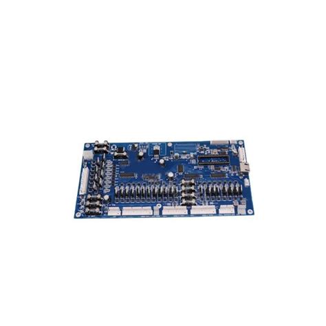
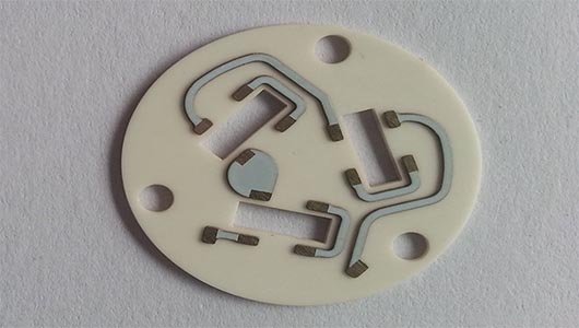
Ceramic pcb fabrication
Advantages Of Ceramic PCB Fabrication Over Traditional PCBs
When it comes to the world of printed circuit boards (PCBs), the choice of materials can make a significant difference in performance, durability, and overall efficiency. While traditional PCBs, typically made from materials like FR4, have been the industry standard for years, ceramic PCBs are increasingly gaining traction. So, what makes ceramic PCB fabrication stand out from the crowd? Let’s dive into the advantages that ceramic PCBs offer over their traditional counterparts.
First and foremost, one of the most compelling benefits of ceramic PCBs is their superior thermal conductivity.
Unlike traditional PCBs, which can struggle with heat dissipation, ceramic PCBs excel in this area. This is particularly important in high-power applications where managing heat is crucial to maintaining performance and preventing damage. With ceramic PCBs, the heat generated by electronic components is efficiently spread out and dissipated, reducing the risk of overheating and extending the lifespan of the device.
In addition to their excellent thermal properties, ceramic PCBs also boast impressive mechanical strength.
Traditional PCBs can be somewhat fragile, especially when subjected to mechanical stress or extreme environmental conditions. Ceramic PCBs, on the other hand, are known for their robustness and durability. They can withstand higher levels of mechanical stress, making them ideal for applications that require a high degree of reliability and longevity. Whether it’s in aerospace, automotive, or industrial settings, ceramic PCBs can handle the rigors of demanding environments with ease.
Another advantage worth mentioning is the high-frequency performance of ceramic PCBs.
Traditional PCBs can suffer from signal loss and interference at high frequencies, which can be a significant drawback in applications like telecommunications and RF (radio frequency) technology. Ceramic materials, however, have excellent dielectric properties, which means they can support high-frequency signals with minimal loss and interference. This makes ceramic PCBs a go-to choice for high-frequency applications where signal integrity is paramount.
Moreover, ceramic PCBs offer a higher degree of miniaturization compared to traditional PCBs.
As electronic devices continue to shrink in size, the need for compact and efficient circuit boards becomes more pressing. Ceramic PCBs can be manufactured with finer lines and spaces, allowing for more components to be packed into a smaller area. This is a game-changer for industries like consumer electronics, where space is at a premium and every millimeter counts.
Furthermore, ceramic PCBs are highly resistant to chemical corrosion and moisture.
Traditional PCBs can degrade over time when exposed to harsh chemicals or humid environments, leading to potential failures and costly repairs. Ceramic materials, however, are inherently resistant to these factors, ensuring long-term reliability and stability. This makes ceramic PCBs an excellent choice for applications in harsh or corrosive environments, such as medical devices or outdoor equipment.
Lastly, it’s worth noting that ceramic PCBs are environmentally friendly.
The materials used in ceramic PCB fabrication are generally non-toxic and can be more easily recycled compared to traditional PCB materials. As the world becomes increasingly conscious of environmental impact, the eco-friendly nature of ceramic PCBs is an added bonus that can’t be overlooked.
In conclusion, while traditional PCBs have served us well for many years, the advantages of ceramic PCB fabrication are hard to ignore. From superior thermal conductivity and mechanical strength to high-frequency performance and miniaturization, ceramic PCBs offer a host of benefits that make them an attractive option for a wide range of applications. As technology continues to evolve, it’s clear that ceramic PCBs are poised to play a significant role in the future of electronic design and manufacturing.
Key Steps In The Ceramic PCB Manufacturing Process
Ceramic PCB fabrication is a fascinating process that combines advanced technology with meticulous craftsmanship. If you’ve ever wondered how these high-performance circuit boards come to life, you’re in for a treat. Let’s dive into the key steps involved in the manufacturing process, and I’ll guide you through it in a way that’s easy to understand.
First things first, it all starts with the selection of the ceramic material.
Unlike traditional PCBs that use fiberglass or plastic substrates, ceramic PCBs are made from materials like alumina, aluminum nitride, or beryllium oxide. These materials are chosen for their excellent thermal conductivity and electrical insulation properties. Once the material is selected, it’s time to move on to the next step.
The ceramic substrate is then cut into the desired shape and size.
This is usually done using a laser cutter or a diamond saw, ensuring precision and accuracy. After cutting, the edges of the substrate are often smoothed out to remove any roughness, which helps in the subsequent steps.
Next up is the cleaning process.
The ceramic substrate needs to be thoroughly cleaned to remove any dust, debris, or contaminants. This is crucial because even the tiniest particle can affect the performance of the final product. Typically, the substrate is cleaned using ultrasonic cleaning methods, which involve immersing it in a cleaning solution and using high-frequency sound waves to dislodge any particles.
Once the substrate is squeaky clean, it’s time for the metallization process.
This involves applying a thin layer of metal, usually copper, onto the surface of the ceramic. The metal layer serves as the conductive pathway for the electrical signals. There are several methods to achieve this, including screen printing, sputtering, and electroplating. Each method has its own advantages and is chosen based on the specific requirements of the PCB.
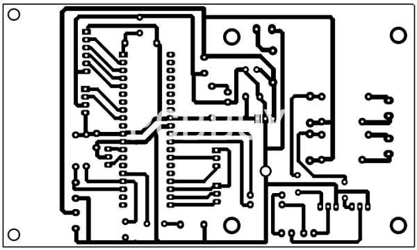
After metallization, the next step is to create the circuit pattern.
This is done using a process called photolithography. A photosensitive material, known as a photoresist, is applied to the metal layer. The desired circuit pattern is then transferred onto the photoresist using ultraviolet light. The exposed areas of the photoresist harden, while the unexposed areas remain soft and can be washed away, revealing the metal underneath.
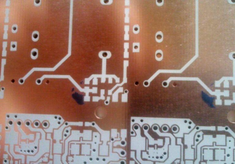
With the circuit pattern in place, it’s time for the etching process.
The substrate is immersed in an etching solution that removes the unwanted metal, leaving behind the desired circuit pattern. This step requires a lot of precision, as any mistakes can lead to faulty circuits.
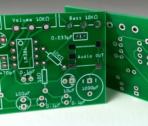
Once the etching is complete, the next step is to apply a protective layer, usually a solder mask, to the PCB.
This layer helps protect the circuit from environmental factors like moisture and dust, and also prevents short circuits. The solder mask is applied using a screen printing process and then cured using heat or ultraviolet light.
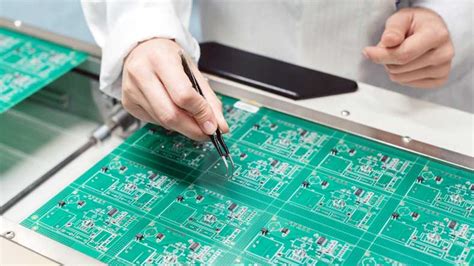
Finally, the PCB undergoes a series of inspections and tests to ensure it meets all the required specifications.
This includes visual inspections, electrical testing, and sometimes even X-ray inspections to check for any hidden defects. Once the PCB passes all the tests, it’s ready to be shipped out and used in various high-performance applications.
And there you have it! The journey from a simple ceramic substrate to a fully functional PCB is quite intricate, but each step is crucial in ensuring the final product is reliable and efficient. Whether it’s for aerospace, medical devices, or high-frequency applications, ceramic PCBs are a testament to the marvels of modern engineering.
Applications Of Ceramic PCBs In High-Performance Electronics
Ceramic PCBs are like the unsung heroes of high-performance electronics. You might not hear about them as often as their fiberglass counterparts, but they play a crucial role in some of the most demanding applications out there. So, what makes ceramic PCBs so special, and where exactly are they used? Let’s dive into the fascinating world of ceramic PCB applications and see why they’re indispensable in high-performance electronics.
First off, ceramic PCBs are known for their excellent thermal conductivity.
This means they can efficiently dissipate heat, which is a big deal in high-power applications. Think about power electronics, where components can get really hot. Traditional PCBs might struggle to keep things cool, but ceramic PCBs handle the heat like a pro. This makes them perfect for use in power modules, LED lighting, and even solar inverters. In these applications, managing heat is crucial for maintaining performance and longevity, and ceramic PCBs deliver on that front.
Moreover, ceramic PCBs are incredibly durable.
They can withstand harsh environments, including extreme temperatures and high levels of mechanical stress. This durability makes them ideal for aerospace and military applications. Imagine the electronics in a fighter jet or a satellite. These devices need to perform flawlessly under extreme conditions, and ceramic PCBs provide the reliability required. They can endure the rigors of space travel or the intense vibrations of a jet engine without breaking a sweat.
In addition to their thermal and mechanical properties, ceramic PCBs offer excellent electrical insulation.
This is particularly important in high-frequency applications, such as RF and microwave circuits. These circuits are used in everything from radar systems to telecommunications equipment. The high dielectric strength of ceramic materials ensures that the signals remain clear and free from interference. This is crucial for maintaining the integrity of the data being transmitted, whether it’s a radar signal or a phone call.
Another exciting application of ceramic PCBs is in medical devices.
Here, the stakes are incredibly high. Devices like pacemakers, defibrillators, and hearing aids need to be both reliable and biocompatible. Ceramic PCBs fit the bill perfectly. They are not only robust and reliable but also safe for use in the human body. This makes them an excellent choice for life-saving medical electronics, where failure is not an option.
Furthermore, the miniaturization trend in electronics has also benefited from ceramic PCBs.
As devices get smaller and more powerful, the need for compact, high-performance components has skyrocketed. Ceramic PCBs can be manufactured with very fine features, allowing for the integration of more components in a smaller space. This is particularly useful in consumer electronics, where space is at a premium. Think about your smartphone or smartwatch. These devices pack a lot of functionality into a tiny form factor, and ceramic PCBs help make that possible.
In conclusion, ceramic PCBs are a cornerstone of high-performance electronics. Their excellent thermal conductivity, durability, electrical insulation, and miniaturization capabilities make them indispensable in a wide range of applications. From power electronics and aerospace to medical devices and consumer gadgets, ceramic PCBs are quietly powering some of the most advanced technologies we rely on every day. So, the next time you marvel at the performance of your favorite high-tech device, remember that a ceramic PCB might just be working its magic behind the scenes.
Innovations In Ceramic PCB Materials And Technologies
Ceramic PCB fabrication has come a long way, and the innovations in materials and technologies are nothing short of fascinating. If you’re into electronics or just curious about how things work, you’ll find this topic pretty intriguing. So, let’s dive into the world of ceramic PCBs and see what’s new and exciting.
First off, let’s talk about why ceramic PCBs are such a big deal.
Traditional PCBs, made from materials like FR4, are great for many applications, but they have their limitations. Ceramic PCBs, on the other hand, offer superior thermal conductivity, better mechanical strength, and excellent electrical insulation. These properties make them ideal for high-power and high-frequency applications, such as LED lighting, power electronics, and RF communication devices.
One of the most significant innovations in ceramic PCB materials is the development of new ceramic substrates.
Alumina (Al2O3) has been the go-to material for a long time, but now we’re seeing the rise of aluminum nitride (AlN) and silicon nitride (Si3N4). These materials offer even better thermal performance and mechanical properties. For instance, AlN has a thermal conductivity that’s about ten times higher than alumina, making it perfect for applications where heat dissipation is critical.
Another exciting development is the use of Low-Temperature Co-fired Ceramics (LTCC) and High-Temperature Co-fired Ceramics (HTCC).
These technologies allow for the integration of multiple layers of ceramic and metal, creating complex, multi-layered PCBs. LTCC, in particular, is gaining popularity because it can be processed at lower temperatures, reducing manufacturing costs and allowing for the use of a wider range of materials.
Speaking of manufacturing, the fabrication process for ceramic PCBs has also seen some impressive advancements.
Traditional methods like thick-film and thin-film deposition are still in use, but new techniques are making waves. One such technique is Direct Bonded Copper (DBC), where a layer of copper is directly bonded to the ceramic substrate. This method offers excellent thermal and electrical performance, making it ideal for high-power applications.
Another innovative fabrication method is Laser Direct Structuring (LDS).
This technique uses a laser to create the circuit pattern directly on the ceramic substrate, eliminating the need for masks and etching processes. LDS offers high precision and flexibility, making it suitable for complex and miniaturized designs.
Moreover, the advent of 3D printing technology has opened up new possibilities in ceramic PCB fabrication.
3D printing allows for the creation of intricate and customized designs that were previously impossible or too costly to produce. This technology is still in its early stages, but it holds great promise for the future of ceramic PCBs.
In addition to these material and technological advancements, there’s also a growing focus on sustainability. Manufacturers are increasingly looking for ways to reduce waste and energy consumption in the fabrication process. For example, some companies are exploring the use of recyclable materials and more energy-efficient production methods.
All these innovations are not just about making better PCBs; they’re about pushing the boundaries of what’s possible in electronics. As we continue to demand more from our devices—higher performance, greater reliability, and smaller sizes—ceramic PCBs will play an increasingly important role. So, whether you’re an engineer, a hobbyist, or just someone who loves tech, it’s worth keeping an eye on this exciting field. The future of ceramic PCB fabrication is bright, and who knows what amazing innovations are just around the corner?