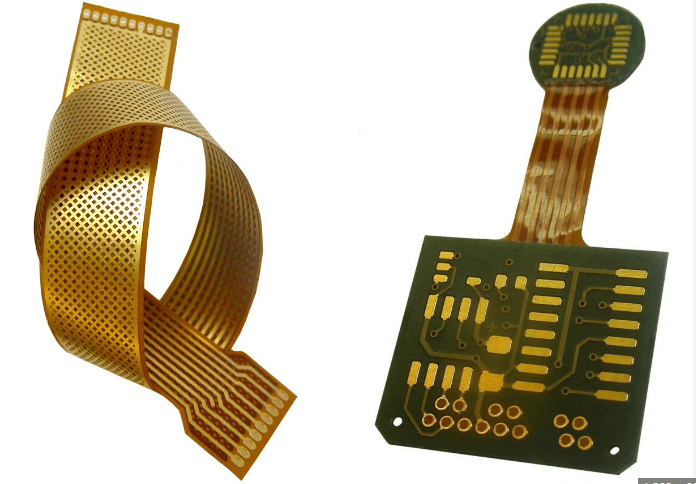
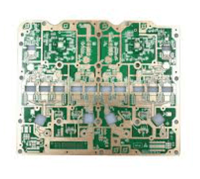
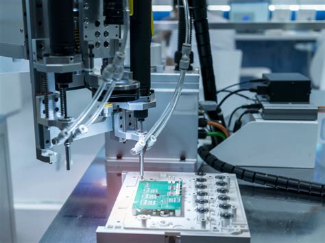
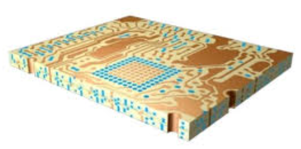
Ceramic pcb multilayer
Advantages Of Using Ceramic PCB Multilayer In High-Frequency Applications
Ceramic PCB multilayer technology has emerged as a pivotal innovation in the realm of high-frequency applications, offering a multitude of advantages that make it an indispensable choice for engineers and designers. One of the primary benefits of using ceramic PCB multilayer in high-frequency applications is its exceptional thermal conductivity. Unlike traditional materials, ceramic substrates can efficiently dissipate heat, thereby ensuring the stability and longevity of electronic components. This characteristic is particularly crucial in high-frequency circuits, where excessive heat can lead to performance degradation and potential failure.
In addition to superior thermal management, ceramic PCB multilayer technology boasts remarkable electrical insulation properties.
The inherent dielectric strength of ceramic materials minimizes the risk of electrical interference, which is a common challenge in high-frequency applications. This ensures that signals remain clear and uncorrupted, thereby enhancing the overall performance and reliability of the electronic system. Furthermore, the low dielectric constant of ceramic substrates contributes to reduced signal loss, which is essential for maintaining signal integrity at high frequencies.
Another significant advantage of ceramic PCB multilayer technology is its mechanical robustness.
Ceramic materials are known for their high strength and durability, which makes them resistant to mechanical stresses and environmental factors such as moisture and temperature fluctuations. This robustness translates to enhanced reliability and longevity of the electronic devices, making ceramic PCBs an ideal choice for applications that demand high performance under challenging conditions.
Moreover, the miniaturization potential offered by ceramic PCB multilayer technology cannot be overlooked.
The ability to stack multiple layers of circuitry within a compact footprint allows for the design of smaller, more efficient electronic devices. This is particularly beneficial in high-frequency applications where space constraints are a common concern. The compact nature of ceramic multilayer PCBs also facilitates the integration of more complex circuitry, thereby enabling the development of advanced electronic systems with enhanced functionality.
Transitioning to the aspect of manufacturing precision, ceramic PCB multilayer technology allows for the creation of intricate and highly accurate circuit patterns.
The precision in manufacturing ensures that the electrical characteristics of the circuits are consistent and reliable, which is paramount in high-frequency applications where even minor deviations can significantly impact performance. Additionally, the compatibility of ceramic substrates with various metallization processes enables the use of different conductive materials, further enhancing the versatility and performance of the PCBs.
Furthermore, the environmental stability of ceramic materials is another noteworthy advantage.
Ceramic PCBs exhibit excellent resistance to chemical corrosion and are less susceptible to environmental degradation compared to their traditional counterparts. This makes them suitable for use in harsh environments where exposure to chemicals, humidity, and extreme temperatures is a concern. The environmental stability of ceramic PCBs ensures that they maintain their performance and reliability over extended periods, thereby reducing the need for frequent replacements and maintenance.
In conclusion, the advantages of using ceramic PCB multilayer technology in high-frequency applications are manifold. From superior thermal management and electrical insulation to mechanical robustness and miniaturization potential, ceramic PCBs offer a comprehensive solution that addresses the unique challenges of high-frequency circuits. The precision in manufacturing and environmental stability further enhance their appeal, making them a preferred choice for engineers and designers seeking to develop reliable, high-performance electronic systems. As technology continues to advance, the role of ceramic PCB multilayer technology in high-frequency applications is poised to become even more significant, driving innovation and excellence in the field of electronics.
Manufacturing Process Of Ceramic PCB Multilayer: A Step-By-Step Guide
The manufacturing process of ceramic PCB multilayer involves a series of meticulously coordinated steps, each contributing to the creation of a robust and efficient electronic component. This process begins with the selection of high-quality ceramic materials, typically alumina or aluminum nitride, known for their excellent thermal conductivity and electrical insulation properties. These materials are chosen based on the specific requirements of the application, ensuring that the final product meets the necessary performance standards.
Once the appropriate ceramic material is selected, it is processed into thin sheets or substrates.
These substrates serve as the foundational layers of the multilayer PCB. The next step involves the application of conductive patterns onto these ceramic substrates. This is achieved through a process known as screen printing, where a conductive paste, usually composed of metals like silver, gold, or copper, is applied to the substrate in the desired pattern. The screen printing process must be precise, as any deviation can affect the performance of the final product.
Following the application of the conductive patterns, the substrates undergo a drying process to remove any solvents present in the conductive paste.
This is typically done in a controlled environment to ensure uniform drying and to prevent any defects. After drying, the substrates are subjected to a high-temperature firing process, which serves to sinter the conductive paste, thereby forming a solid and reliable conductive layer. This firing process is critical, as it determines the electrical and mechanical properties of the conductive patterns.
With the conductive layers in place, the next step involves stacking the individual ceramic substrates to form a multilayer structure.
This stacking process requires precise alignment to ensure that the conductive patterns on each layer are correctly positioned relative to one another. Misalignment at this stage can lead to short circuits or other electrical issues in the final product. To secure the stacked layers, a lamination process is employed, where the layers are pressed together under high pressure and temperature. This not only bonds the layers but also ensures that the multilayer structure is compact and stable.
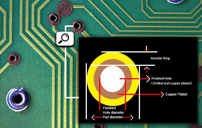
Once the multilayer structure is formed, vias or through-holes are created to establish electrical connections between the different layers.
This is typically done using laser drilling or mechanical drilling techniques, depending on the specific requirements of the PCB. The vias are then filled with a conductive material, usually a metal paste, to ensure reliable electrical connectivity. This step is crucial for the overall functionality of the multilayer PCB, as it enables the interconnection of the various conductive layers.
After the vias are filled, the multilayer PCB undergoes a final firing process to sinter the conductive material in the vias and to further solidify the entire structure.
This final firing ensures that all the layers are securely bonded and that the electrical connections are robust. Following this, the PCB is subjected to a series of inspections and tests to verify its electrical performance and structural integrity. Any defects identified during this stage are addressed to ensure that the final product meets the required specifications.
In conclusion, the manufacturing process of ceramic PCB multilayer is a complex and precise operation that involves multiple steps, each critical to the performance and reliability of the final product. From the selection of high-quality ceramic materials to the final inspection and testing, each stage must be carefully controlled to produce a PCB that meets the stringent demands of modern electronic applications.
Thermal Management Solutions With Ceramic PCB Multilayer Technology
Ceramic PCB multilayer technology has emerged as a pivotal solution in the realm of thermal management, addressing the growing demands of high-performance electronic devices. As electronic components continue to shrink in size while increasing in power density, efficient thermal management becomes crucial to ensure reliability and longevity. Ceramic PCBs, particularly those with multilayer configurations, offer a robust platform to dissipate heat effectively, thereby enhancing the performance and durability of electronic systems.
One of the primary advantages of ceramic PCB multilayer technology is its superior thermal conductivity.
Traditional PCB materials, such as FR4, often struggle to manage heat dissipation in high-power applications. In contrast, ceramic substrates, including alumina (Al2O3) and aluminum nitride (AlN), exhibit excellent thermal conductivity properties. This inherent characteristic allows ceramic PCBs to efficiently transfer heat away from critical components, reducing the risk of thermal-related failures. Consequently, devices utilizing ceramic multilayer PCBs can operate at higher power levels without compromising their operational integrity.
Moreover, ceramic PCB multilayer technology offers enhanced mechanical stability and reliability.
The ceramic materials used in these PCBs are inherently rigid and resistant to thermal expansion, which is a common issue in traditional PCB materials. This stability ensures that the multilayer structure remains intact even under extreme thermal cycling conditions, thereby preventing delamination and other mechanical failures. Additionally, the high dielectric strength of ceramic materials provides excellent electrical insulation, further contributing to the overall reliability of the electronic system.
In addition to thermal and mechanical benefits, ceramic PCB multilayer technology also enables greater design flexibility. The multilayer configuration allows for the integration of multiple circuit layers within a single PCB, facilitating complex circuit designs and higher component density. This capability is particularly advantageous in applications where space is at a premium, such as in aerospace, medical devices, and advanced communication systems. By incorporating multiple layers, designers can achieve more compact and efficient layouts, ultimately leading to smaller and lighter electronic devices.
Furthermore, the use of ceramic materials in multilayer PCBs enhances their performance in harsh environments.
Ceramic substrates are inherently resistant to moisture, chemicals, and radiation, making them ideal for applications in extreme conditions. For instance, in aerospace and defense industries, where electronic systems are exposed to high levels of radiation and temperature fluctuations, ceramic multilayer PCBs provide a reliable solution. Similarly, in medical devices, where sterilization processes involve exposure to harsh chemicals and high temperatures, ceramic PCBs ensure the longevity and reliability of the electronic components.
The manufacturing process of ceramic PCB multilayer technology also contributes to its effectiveness in thermal management.
Advanced fabrication techniques, such as low-temperature co-fired ceramics (LTCC) and high-temperature co-fired ceramics (HTCC), allow for precise control over the material properties and layer configurations. These techniques enable the production of multilayer PCBs with tailored thermal and electrical characteristics, meeting the specific requirements of various applications. Additionally, the ability to integrate passive components, such as resistors and capacitors, directly into the ceramic substrate further enhances the functionality and performance of the multilayer PCB.
In conclusion, ceramic PCB multilayer technology represents a significant advancement in thermal management solutions for high-performance electronic devices. Its superior thermal conductivity, mechanical stability, design flexibility, and resilience in harsh environments make it an ideal choice for a wide range of applications. As electronic devices continue to evolve, the adoption of ceramic multilayer PCBs will undoubtedly play a crucial role in meeting the increasing demands for efficient thermal management and reliable performance.
Comparing Ceramic PCB Multilayer To Traditional PCB Materials
Ceramic PCB multilayer technology has emerged as a significant advancement in the field of electronic circuit design, offering distinct advantages over traditional PCB materials. To understand the benefits and limitations of ceramic PCB multilayer technology, it is essential to compare it with conventional PCB materials such as FR-4, a widely used fiberglass-reinforced epoxy laminate.
One of the primary advantages of ceramic PCB multilayer technology is its superior thermal conductivity.
Traditional PCB materials like FR-4 have relatively low thermal conductivity, which can lead to overheating issues in high-power applications. In contrast, ceramic materials such as aluminum oxide (Al2O3) and aluminum nitride (AlN) exhibit excellent thermal conductivity, allowing for efficient heat dissipation. This characteristic makes ceramic PCBs particularly suitable for applications that require high thermal management, such as power electronics, LED lighting, and RF modules.
Moreover, ceramic PCBs offer enhanced mechanical stability and reliability.
Traditional PCBs can suffer from issues such as delamination and warping under thermal stress, which can compromise the integrity of the circuit. Ceramic materials, however, are inherently more robust and resistant to thermal expansion and contraction. This stability ensures that ceramic PCBs maintain their structural integrity even under extreme temperature variations, thereby enhancing the longevity and reliability of the electronic devices they support.
In addition to thermal and mechanical advantages, ceramic PCB multilayer technology also provides superior electrical performance. The dielectric properties of ceramic materials are significantly better than those of traditional PCB materials. This results in lower signal loss and higher signal integrity, which is crucial for high-frequency applications. Consequently, ceramic PCBs are often preferred in industries such as telecommunications, aerospace, and medical devices, where precise and reliable signal transmission is paramount.
Despite these advantages, it is important to acknowledge the limitations of ceramic PCB multilayer technology.
One of the most significant drawbacks is the cost. Ceramic materials and the processes involved in manufacturing ceramic PCBs are generally more expensive than those for traditional PCBs. This higher cost can be a deterrent for applications where budget constraints are a primary concern. However, for high-performance applications where the benefits of ceramic PCBs outweigh the cost considerations, the investment is often justified.
Another limitation is the complexity of the manufacturing process.
Producing ceramic PCBs involves specialized techniques such as tape casting, lamination, and sintering, which require advanced equipment and expertise. This complexity can lead to longer lead times and higher production costs compared to traditional PCB manufacturing processes. Nevertheless, advancements in manufacturing technologies are gradually mitigating these challenges, making ceramic PCBs more accessible to a broader range of applications.
Furthermore, while ceramic PCBs excel in high-temperature and high-frequency environments,
they may not be necessary for all applications. For low-power, low-frequency, and cost-sensitive projects, traditional PCB materials like FR-4 may still be the more practical choice. Therefore, the decision to use ceramic PCB multilayer technology should be based on a thorough assessment of the specific requirements and constraints of the application.
In conclusion, ceramic PCB multilayer technology offers significant advantages in terms of thermal management, mechanical stability, and electrical performance compared to traditional PCB materials. However, these benefits come with higher costs and manufacturing complexities. As such, the choice between ceramic and traditional PCBs should be carefully considered based on the specific needs of the application, balancing performance requirements with budgetary constraints.