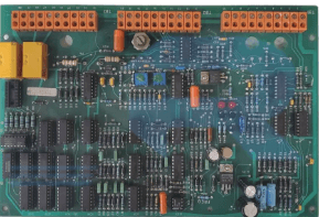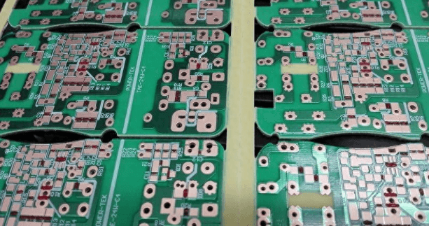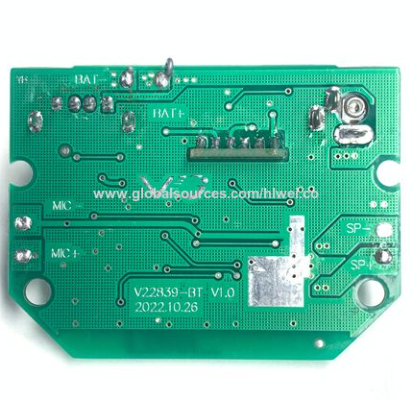
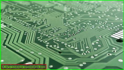
Ceramic pcb prototype
Advantages Of Using Ceramic PCB Prototypes In High-Frequency Applications
Ceramic PCB prototypes have emerged as a pivotal component in the realm of high-frequency applications, offering a multitude of advantages that make them an attractive choice for engineers and designers. As the demand for high-performance electronic devices continues to escalate, the need for reliable and efficient circuit boards becomes increasingly critical. Ceramic PCBs, with their unique properties, provide a solution that addresses many of the challenges associated with high-frequency applications.
One of the primary advantages of ceramic PCBs is their exceptional thermal conductivity.
Unlike traditional materials such as FR-4, ceramics can efficiently dissipate heat, which is crucial in high-frequency applications where components often generate significant amounts of heat. This superior thermal management capability ensures that the electronic components maintain optimal performance and longevity, reducing the risk of overheating and subsequent failure. Consequently, devices that incorporate ceramic PCBs can operate at higher power levels and frequencies without compromising reliability.
In addition to thermal management, ceramic PCBs offer excellent electrical insulation properties
This characteristic is particularly important in high-frequency applications where signal integrity is paramount. The dielectric properties of ceramic materials minimize signal loss and crosstalk, ensuring that the signals remain clear and precise. This results in improved performance and efficiency of the electronic device, making ceramic PCBs an ideal choice for applications such as RF modules, microwave circuits, and high-speed communication systems.
Moreover, ceramic PCBs exhibit remarkable mechanical strength and stability.
Their robust nature allows them to withstand harsh environmental conditions, including extreme temperatures and mechanical stress. This durability is essential for high-frequency applications that often operate in challenging environments, such as aerospace, automotive, and military sectors. The ability of ceramic PCBs to maintain structural integrity under such conditions ensures the reliability and longevity of the electronic devices they support.
Furthermore, the miniaturization of electronic components is a growing trend in the industry, and ceramic PCBs are well-suited to meet this demand.
Their high thermal and electrical performance allows for the integration of smaller components without sacrificing functionality. This capability is particularly beneficial in high-frequency applications where space is often at a premium. The compact nature of ceramic PCBs enables the design of smaller, more efficient devices, which is a significant advantage in today’s fast-paced technological landscape.
In addition to these technical benefits, ceramic PCBs also offer environmental advantages.
They are typically made from non-toxic materials and are more environmentally friendly compared to traditional PCB materials. This aligns with the growing emphasis on sustainability and eco-friendly practices within the electronics industry.
In conclusion, the advantages of using ceramic PCB prototypes in high-frequency applications are manifold. Their superior thermal conductivity, excellent electrical insulation, mechanical strength, and suitability for miniaturization make them an ideal choice for a wide range of high-performance electronic devices. As technology continues to advance and the demand for efficient, reliable, and compact devices grows, ceramic PCBs are poised to play an increasingly important role in meeting these challenges. Their unique properties not only enhance the performance and reliability of electronic devices but also contribute to the broader goals of sustainability and innovation in the industry.
Step-By-Step Guide To Designing A Ceramic PCB Prototype
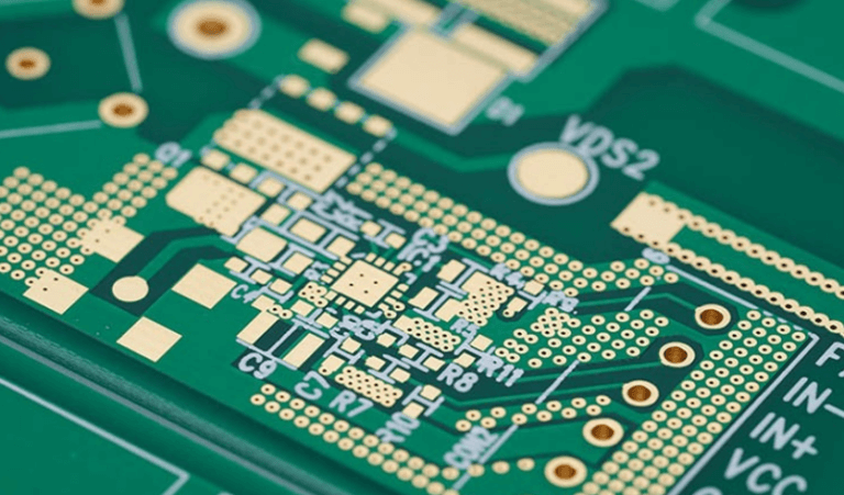
Designing a ceramic PCB prototype involves a meticulous process that requires attention to detail and a comprehensive understanding of both the materials and the technology involved. Ceramic PCBs are renowned for their excellent thermal conductivity, high-frequency performance, and superior mechanical strength, making them ideal for applications in demanding environments. To begin the design process, it is essential to first understand the specific requirements of the application for which the PCB is being developed. This involves identifying the electrical, thermal, and mechanical demands that the PCB must meet, as well as any size or weight constraints.
Once the requirements are clearly defined, the next step is to select the appropriate ceramic material.
Common materials include alumina, aluminum nitride, and beryllium oxide, each offering distinct properties. Alumina is widely used due to its cost-effectiveness and good thermal performance, while aluminum nitride provides superior thermal conductivity, making it suitable for high-power applications. Beryllium oxide, although less common due to its toxicity, offers excellent thermal and electrical properties. The choice of material will significantly impact the performance and cost of the final product.
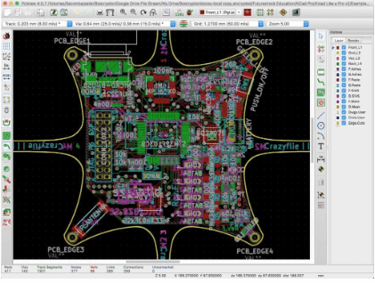
With the material selected, the design process can proceed to the layout phase.
This involves creating a schematic diagram that outlines the electrical connections and components of the PCB. Advanced software tools are typically employed to facilitate this process, allowing designers to simulate the circuit and optimize the layout for performance and manufacturability. During this phase, it is crucial to consider factors such as trace width, spacing, and the placement of components to ensure efficient heat dissipation and signal integrity.
Following the schematic design, the next step is to create the physical layout of the PCB.
This involves translating the schematic into a physical representation that can be manufactured. The layout must account for the unique properties of ceramic materials, such as their brittleness and thermal expansion characteristics. Designers must ensure that the layout minimizes stress concentrations and accommodates any potential thermal expansion to prevent cracking or warping during operation.
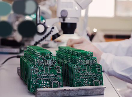
Once the layout is finalized, the prototype can be manufactured.
This typically involves a process known as thick-film or thin-film technology, where conductive, resistive, and dielectric layers are deposited onto the ceramic substrate. Thick-film technology is often preferred for its cost-effectiveness and versatility, while thin-film technology offers higher precision and performance. The choice between these methods will depend on the specific requirements of the application and the desired characteristics of the PCB.
After manufacturing, the prototype undergoes rigorous testing to ensure it meets the specified requirements
This includes electrical testing to verify circuit functionality, thermal testing to assess heat dissipation capabilities, and mechanical testing to evaluate durability under stress. Any issues identified during testing must be addressed through iterative design modifications and re-testing until the prototype meets all performance criteria.
In conclusion, designing a ceramic PCB prototype is a complex process that requires careful consideration of material properties, design constraints, and manufacturing techniques. By following a systematic approach and leveraging advanced design tools, engineers can develop high-performance ceramic PCBs that meet the demanding requirements of modern electronic applications. This step-by-step guide provides a foundational understanding of the process, enabling designers to navigate the challenges and opportunities presented by ceramic PCB technology.
Comparing Ceramic PCB Prototypes To Traditional FR4 PCBs
In the realm of electronics, the choice of substrate material for printed circuit boards (PCBs) plays a crucial role in determining the performance, reliability, and longevity of electronic devices. Among the various materials available, ceramic PCBs and traditional FR4 PCBs are two prominent options, each with distinct characteristics and advantages. Understanding the differences between these two types of PCBs is essential for engineers and designers aiming to optimize their electronic applications.
Ceramic PCBs, often made from materials such as alumina or aluminum nitride, are renowned for their exceptional thermal conductivity and mechanical strength.
These properties make them particularly suitable for high-power applications where efficient heat dissipation is critical. In contrast, traditional FR4 PCBs, composed of woven fiberglass cloth with an epoxy resin binder, are more commonly used in general electronic applications due to their cost-effectiveness and versatility. However, they fall short in thermal management compared to their ceramic counterparts.
One of the primary advantages of ceramic PCBs is their ability to operate in extreme temperature environments.
The inherent thermal stability of ceramic materials allows these PCBs to withstand temperatures that would typically degrade or damage FR4 boards. This makes ceramic PCBs ideal for applications in aerospace, automotive, and industrial sectors, where devices are often exposed to harsh conditions. Moreover, the high thermal conductivity of ceramic substrates ensures efficient heat dissipation, reducing the risk of overheating and enhancing the overall reliability of the electronic components.
In addition to thermal performance, ceramic PCBs offer superior electrical insulation properties.
The dielectric strength of ceramic materials is significantly higher than that of FR4, which translates to better performance in high-frequency applications. This characteristic is particularly beneficial in RF and microwave circuits, where signal integrity is paramount. Furthermore, the low dielectric constant of ceramic substrates minimizes signal loss, thereby improving the efficiency of high-speed data transmission.
Despite these advantages, ceramic PCBs are not without their drawbacks.
The manufacturing process for ceramic PCBs is more complex and costly compared to FR4 boards. The materials used in ceramic PCBs are inherently more expensive, and the production techniques require specialized equipment and expertise. Consequently, the initial investment for ceramic PCB prototypes can be significantly higher, which may deter some manufacturers from adopting this technology for cost-sensitive projects.
On the other hand, traditional FR4 PCBs remain a popular choice due to their affordability and ease of fabrication.
The well-established manufacturing processes for FR4 boards allow for rapid prototyping and mass production, making them suitable for a wide range of consumer electronics. Additionally, the flexibility of FR4 materials enables the creation of multilayer PCBs, which are essential for complex circuit designs.
In conclusion, the decision between ceramic PCB prototypes and traditional FR4 PCBs hinges on the specific requirements of the application.
While ceramic PCBs offer unparalleled thermal and electrical performance, their higher cost and manufacturing complexity may not be justified for all projects. Conversely, FR4 PCBs provide a cost-effective solution for general-purpose electronics but may fall short in demanding environments. Ultimately, a thorough evaluation of the application’s needs, budget constraints, and performance expectations is necessary to make an informed choice between these two types of PCBs.
Innovations In Ceramic PCB Prototype Manufacturing Techniques
Ceramic printed circuit boards (PCBs) have emerged as a pivotal component in the electronics industry, particularly in applications requiring high thermal conductivity and superior electrical insulation. As the demand for more efficient and reliable electronic devices continues to grow, innovations in ceramic PCB prototype manufacturing techniques have become increasingly significant. These advancements not only enhance the performance of electronic devices but also contribute to the miniaturization and durability of modern technology.
One of the most notable innovations in ceramic PCB manufacturing is the development of Low-Temperature Co-fired Ceramics (LTCC).
This technique involves the co-firing of multiple layers of ceramic and metal at relatively low temperatures, typically below 900°C. LTCC technology allows for the integration of passive components such as resistors, capacitors, and inductors directly into the ceramic substrate. This integration results in a more compact design, reducing the overall size and weight of the electronic device. Moreover, LTCC offers excellent thermal management properties, making it ideal for high-frequency and high-power applications.
In addition to LTCC, another significant advancement is the use of Direct Bonded Copper (DBC) substrates.
DBC technology involves bonding a layer of copper directly onto a ceramic substrate, typically aluminum oxide or aluminum nitride. This method provides exceptional thermal conductivity and mechanical strength, which are crucial for power electronics and automotive applications. The direct bonding process ensures a robust connection between the copper and ceramic, enhancing the reliability and longevity of the PCB. Furthermore, DBC substrates are capable of handling high current loads, making them suitable for applications such as electric vehicles and renewable energy systems.
The advent of Additive Manufacturing (AM) techniques has also revolutionized ceramic PCB prototyping.
AM, commonly known as 3D printing, allows for the precise deposition of ceramic materials layer by layer, enabling the creation of complex geometries that were previously unattainable with traditional manufacturing methods. This capability is particularly beneficial for producing customized PCBs with intricate designs and specific performance characteristics. Additionally, AM reduces material waste and shortens production lead times, offering a more sustainable and cost-effective solution for prototype development.
Moreover, advancements in laser processing technology have significantly improved the precision and efficiency of ceramic PCB manufacturing.
Laser drilling and cutting techniques enable the creation of microvias and fine features with high accuracy, essential for the miniaturization of electronic components. The use of lasers also minimizes mechanical stress on the ceramic substrate, reducing the risk of damage during the manufacturing process. This precision is crucial for applications in telecommunications, aerospace, and medical devices, where reliability and performance are paramount.
In conclusion, the continuous evolution of ceramic PCB prototype manufacturing techniques is driving the electronics industry towards more efficient, reliable, and compact solutions. Innovations such as LTCC, DBC substrates, additive manufacturing, and laser processing are at the forefront of this transformation, offering enhanced thermal management, mechanical strength, and design flexibility. As these technologies continue to advance, they will undoubtedly play a critical role in meeting the ever-increasing demands of modern electronic applications, paving the way for future developments in the field.
Cost-Effective Strategies For Developing Ceramic PCB Prototypes
Developing ceramic PCB prototypes can be a complex and costly endeavor, yet with the right strategies, it is possible to manage expenses effectively while ensuring high-quality outcomes. Ceramic PCBs, known for their excellent thermal conductivity and electrical insulation properties, are increasingly used in high-performance applications. However, the unique materials and processes involved in their production can lead to significant costs. Therefore, adopting cost-effective strategies is crucial for businesses aiming to innovate without overspending.
To begin with, selecting the appropriate ceramic material is a fundamental step in controlling costs.
Alumina and aluminum nitride are popular choices, each offering distinct advantages. Alumina is more cost-effective and provides good thermal performance, making it suitable for many applications. On the other hand, aluminum nitride offers superior thermal conductivity but at a higher price point. By carefully evaluating the specific requirements of the project, such as thermal management needs and budget constraints, developers can make informed decisions that balance performance with cost.
Another strategy involves optimizing the design process.
Utilizing advanced design software can significantly reduce the time and resources required to develop a prototype. These tools allow for precise modeling and simulation, enabling engineers to identify potential issues early in the design phase. By addressing these problems before physical production begins, companies can avoid costly revisions and material waste. Furthermore, engaging in thorough design reviews and iterative testing can enhance the reliability of the prototype, ultimately leading to a more efficient development process.
In addition to design optimization, leveraging economies of scale can also contribute to cost savings.
While initial prototypes may be produced in small quantities, planning for larger production runs can reduce the per-unit cost. This approach requires careful forecasting and market analysis to ensure that the demand justifies the increased production volume. By aligning production capacity with market needs, companies can achieve a more favorable cost structure.
Moreover, collaborating with experienced manufacturers can provide access to specialized knowledge and resources that may not be available in-house.
These partnerships can lead to more efficient production processes and better material sourcing, ultimately reducing costs. Manufacturers with expertise in ceramic PCBs can offer valuable insights into process improvements and cost-saving opportunities. Establishing strong relationships with these partners can also lead to more favorable pricing and terms, further enhancing cost-effectiveness.
Additionally, exploring alternative fabrication techniques can yield significant savings.
For instance, using additive manufacturing or 3D printing technologies can reduce material waste and lower production costs. These methods allow for greater design flexibility and can be particularly beneficial for complex or custom designs. By staying abreast of technological advancements and incorporating innovative production methods, companies can maintain a competitive edge while managing expenses.
Finally, implementing a robust project management framework is essential for controlling costs throughout the development process.
This includes setting clear objectives, timelines, and budgets, as well as regularly monitoring progress and expenditures. Effective project management ensures that resources are allocated efficiently and that any deviations from the plan are promptly addressed. By maintaining a disciplined approach to project execution, companies can minimize unexpected costs and deliver successful ceramic PCB prototypes within budget.
In conclusion, developing ceramic PCB prototypes cost-effectively requires a multifaceted approach that encompasses material selection, design optimization, economies of scale, strategic partnerships, innovative fabrication techniques, and strong project management. By integrating these strategies, businesses can navigate the complexities of ceramic PCB development while achieving their financial and technical objectives.