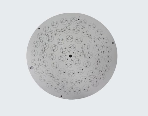
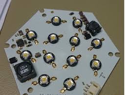
ceramic rf pcb
Advantages Of Using Ceramic RF PCBs In High-Frequency Applications
When it comes to high-frequency applications, the choice of materials for printed circuit boards (PCBs) can make a world of difference. One material that has been gaining traction in this realm is ceramic. Ceramic RF PCBs, or radio frequency printed circuit boards, offer a plethora of advantages that make them particularly well-suited for high-frequency applications. Let’s dive into why these ceramic-based boards are becoming the go-to option for engineers and designers alike.
First and foremost, ceramic RF PCBs excel in thermal management.
High-frequency applications often generate a significant amount of heat, and managing this heat is crucial to maintaining performance and longevity. Ceramic materials have excellent thermal conductivity, which means they can efficiently dissipate heat away from critical components. This not only helps in keeping the system cool but also enhances the overall reliability of the device. Imagine running a high-frequency application without the constant worry of overheating—sounds like a dream, right?
Moreover, ceramic RF PCBs offer superior electrical performance.
The dielectric properties of ceramic materials are far better than those of traditional FR4 materials commonly used in PCBs. This translates to lower signal loss and higher signal integrity, which are essential for high-frequency applications. When you’re dealing with frequencies in the gigahertz range, even the slightest signal degradation can lead to performance issues. Ceramic materials help in maintaining the integrity of these high-frequency signals, ensuring that your application runs smoothly and efficiently.
In addition to thermal and electrical advantages, ceramic RF PCBs are also incredibly durable.
They are resistant to environmental factors such as moisture, chemicals, and extreme temperatures. This makes them ideal for applications that need to operate in harsh conditions. Whether it’s a satellite in space or a communication device in a remote location, ceramic RF PCBs can withstand the rigors of challenging environments. This durability translates to fewer failures and less maintenance, which is always a win in any engineering project.
Another noteworthy benefit is the miniaturization potential that ceramic RF PCBs offer.
As technology advances, there’s a growing demand for smaller, more compact devices. Ceramic materials allow for the creation of thinner and more densely packed PCBs without compromising on performance. This is particularly beneficial in applications like smartphones, medical devices, and IoT gadgets, where space is at a premium. With ceramic RF PCBs, you can pack more functionality into a smaller footprint, making your designs not only more efficient but also more innovative.
Furthermore, ceramic RF PCBs are highly customizable.
They can be tailored to meet specific requirements, whether it’s a unique shape, size, or performance characteristic. This flexibility allows engineers to design PCBs that are perfectly suited to their application’s needs, rather than having to make compromises. Customization can lead to optimized performance, reduced costs, and faster time-to-market, all of which are critical factors in today’s fast-paced tech landscape.
In conclusion, the advantages of using ceramic RF PCBs in high-frequency applications are numerous and compelling. From superior thermal management and electrical performance to exceptional durability and miniaturization potential, ceramic materials offer a robust solution for the challenges posed by high-frequency applications. As technology continues to evolve, it’s clear that ceramic RF PCBs will play an increasingly important role in enabling the next generation of high-frequency devices. So, if you’re working on a high-frequency application, it might be time to consider making the switch to ceramic RF PCBs. You won’t be disappointed.
Manufacturing Process Of Ceramic RF PCBs: A Step-By-Step Guide
When it comes to the world of high-frequency electronics, ceramic RF PCBs are the unsung heroes. These specialized circuit boards are designed to handle the rigors of radio frequency applications, offering superior performance and reliability. But have you ever wondered how these intricate pieces of technology are made? Let’s take a journey through the manufacturing process of ceramic RF PCBs, step by step.
First things first, it all starts with the selection of the ceramic substrate.
Unlike traditional PCBs that use fiberglass or other materials, ceramic RF PCBs rely on ceramic substrates like alumina or aluminum nitride. These materials are chosen for their excellent thermal conductivity and low dielectric loss, which are crucial for high-frequency applications. Once the substrate is selected, it is cut into the desired size and shape, setting the stage for the next steps.
Next up is the application of the conductive layer.
This is where things start to get a bit more technical. A thin layer of metal, usually copper, is deposited onto the ceramic substrate. This can be done through various methods such as screen printing, sputtering, or electroplating. The choice of method depends on the specific requirements of the PCB, including the thickness of the conductive layer and the level of precision needed.
After the conductive layer is applied, it’s time for the photolithography process.
This is where the intricate patterns of the circuit are created. A photosensitive material, known as a photoresist, is applied over the conductive layer. The PCB is then exposed to ultraviolet light through a mask that contains the desired circuit pattern. The areas exposed to the light harden, while the unexposed areas remain soft and can be washed away, revealing the underlying conductive layer in the desired pattern.
With the circuit pattern now in place, the next step is etching.
This involves using a chemical solution to remove the unwanted copper, leaving behind only the desired circuit traces. The etching process must be carefully controlled to ensure that the traces are of the correct width and spacing, as even minor deviations can affect the performance of the RF PCB.
Once the etching is complete, the photoresist is removed, and the PCB undergoes a thorough cleaning process to remove any remaining chemicals or debris.
At this point, the basic structure of the ceramic RF PCB is complete, but there are still a few more steps to go.
The next stage involves the application of a protective layer, often referred to as a solder mask. This layer helps to protect the delicate circuit traces from damage and corrosion. It also helps to prevent solder bridges during the assembly process, ensuring that the components are properly connected.
Finally, the PCB is ready for the addition of components.
This is typically done using surface-mount technology (SMT), where components are placed directly onto the surface of the PCB and soldered into place. The assembled PCB then undergoes rigorous testing to ensure that it meets all performance specifications.
And there you have it! From the selection of the ceramic substrate to the final assembly and testing, the manufacturing process of ceramic RF PCBs is a complex and precise endeavor. Each step is carefully controlled to ensure that the final product can handle the demands of high-frequency applications, making these specialized circuit boards an essential component in the world of modern electronics.
Comparing Ceramic RF PCBs To Traditional FR4 PCBs: Performance And Reliability
When it comes to designing and manufacturing printed circuit boards (PCBs) for radio frequency (RF) applications, the choice of material can significantly impact performance and reliability. Two popular materials in this realm are ceramic and traditional FR4. While both have their merits, understanding the differences between ceramic RF PCBs and FR4 PCBs can help you make an informed decision for your next project.
First off, let’s talk about the basics.
FR4 is a widely-used material in the PCB industry, known for its versatility and cost-effectiveness. It’s made from woven fiberglass cloth with an epoxy resin binder, which gives it decent mechanical strength and electrical insulation properties. On the other hand, ceramic PCBs are made from materials like alumina or aluminum nitride, which offer superior thermal and electrical performance. This fundamental difference in material composition sets the stage for a variety of performance and reliability distinctions.
One of the most significant advantages of ceramic RF PCBs is their excellent thermal conductivity.
Ceramic materials can dissipate heat much more efficiently than FR4, which is crucial in high-power RF applications where excessive heat can lead to performance degradation or even component failure. This means that ceramic PCBs can handle higher power levels without the need for additional cooling mechanisms, making them ideal for applications like power amplifiers and microwave circuits.
In addition to thermal performance, ceramic PCBs also excel in terms of electrical properties.
They have a lower dielectric constant and loss tangent compared to FR4, which translates to better signal integrity and reduced signal loss at high frequencies. This is particularly important in RF applications where maintaining signal fidelity is paramount. With ceramic PCBs, you can achieve higher frequency operation and better overall performance, which can be a game-changer in applications like wireless communication and radar systems.
However, it’s not all sunshine and rainbows with ceramic PCBs.
One of the main drawbacks is cost. Ceramic materials and the processes required to manufacture ceramic PCBs are generally more expensive than those for FR4. This can be a significant consideration, especially for budget-conscious projects or high-volume production runs. Additionally, ceramic PCBs can be more brittle and prone to mechanical damage compared to the more flexible FR4, which can be a concern during handling and assembly.
Despite these challenges, the reliability of ceramic RF PCBs often outweighs the drawbacks.
Their superior thermal and electrical performance can lead to longer-lasting and more reliable products, which can be a critical factor in industries where failure is not an option, such as aerospace and medical devices. Moreover, advancements in manufacturing techniques are gradually reducing the cost and improving the robustness of ceramic PCBs, making them more accessible for a wider range of applications.
In contrast, FR4 PCBs remain a popular choice for many RF applications due to their cost-effectiveness and mechanical robustness. They are easier to manufacture and handle, which can simplify the production process and reduce costs. While they may not offer the same level of performance as ceramic PCBs, they can still be a viable option for lower-frequency applications or where budget constraints are a primary concern.
In conclusion, the choice between ceramic RF PCBs and traditional FR4 PCBs boils down to a trade-off between performance, reliability, and cost. Ceramic PCBs offer superior thermal and electrical properties, making them ideal for high-frequency and high-power applications, albeit at a higher cost and with some mechanical limitations. On the other hand, FR4 PCBs provide a more cost-effective and mechanically robust solution, suitable for a wide range of applications. By carefully considering the specific requirements of your project, you can make an informed decision that balances these factors to achieve the best possible outcome.
Innovations In Ceramic RF PCB Technology For Next-Generation Wireless Communication
Ceramic RF PCBs are making waves in the world of wireless communication, and it’s not hard to see why. As we dive deeper into the era of 5G and beyond, the demand for high-performance, reliable, and efficient communication systems is skyrocketing. This is where ceramic RF PCBs come into play, offering a host of benefits that traditional materials simply can’t match.
First off, let’s talk about the material itself.
Ceramic substrates are known for their excellent thermal properties, which is a game-changer for RF applications. Unlike traditional FR4 materials, ceramics can handle higher temperatures without breaking a sweat. This means that devices can operate at higher power levels and frequencies without the risk of overheating. In a world where every millisecond counts, this thermal stability is crucial for maintaining the integrity and performance of communication systems.
Moreover, ceramic RF PCBs offer superior electrical properties.
The low dielectric constant and loss tangent of ceramic materials ensure minimal signal loss and distortion. This translates to clearer, more reliable communication, which is essential for applications ranging from mobile phones to satellite communications. The high-frequency performance of ceramic substrates makes them ideal for the next generation of wireless technologies, where speed and efficiency are paramount.
Transitioning to the manufacturing process, ceramic RF PCBs are also incredibly versatile.
Advanced manufacturing techniques like Low-Temperature Co-fired Ceramics (LTCC) and High-Temperature Co-fired Ceramics (HTCC) allow for the integration of multiple layers and components into a single, compact package. This not only saves space but also reduces the overall weight of the device, making it more suitable for portable and wearable applications. Additionally, the ability to integrate passive components like resistors, capacitors, and inductors directly into the substrate simplifies the design and enhances the overall performance of the PCB.
Another exciting aspect of ceramic RF PCBs is their durability.
Ceramics are inherently robust and resistant to environmental factors such as moisture, chemicals, and mechanical stress. This makes them ideal for use in harsh environments, whether it’s a satellite orbiting the Earth or a sensor in an industrial setting. The long-term reliability of ceramic RF PCBs ensures that they can withstand the rigors of real-world applications, providing peace of mind for both manufacturers and end-users.
As we look to the future, the potential applications for ceramic RF PCBs are virtually limitless.
From the Internet of Things (IoT) to autonomous vehicles, the need for high-performance, reliable communication systems is only going to grow. Ceramic RF PCBs are poised to play a pivotal role in this evolution, offering the perfect blend of performance, reliability, and versatility.
In conclusion, the innovations in ceramic RF PCB technology are paving the way for the next generation of wireless communication. With their superior thermal and electrical properties, advanced manufacturing techniques, and unparalleled durability, ceramic RF PCBs are set to revolutionize the industry. As we continue to push the boundaries of what’s possible, it’s clear that ceramic RF PCBs will be at the forefront of this exciting journey. So, whether you’re a tech enthusiast or a seasoned professional, keep an eye on this space – the future of wireless communication is brighter than ever, thanks to ceramic RF PCBs.


