Characteristic Impedance Control in PCB Design
Introduction
Printed Circuit Boards (PCBs) are the backbone of modern electronics, enabling the interconnection of various components to form functional circuits. As electronic devices operate at increasingly higher frequencies, signal integrity becomes a critical concern. One of the most important factors affecting signal integrity in high-speed PCB designs is characteristic impedance control.
Characteristic impedance refers to the inherent resistance to the flow of electrical energy along a transmission line. Proper impedance control ensures minimal signal reflections, reduced electromagnetic interference (EMI), and optimal power transfer. This article explores the fundamentals of characteristic impedance, factors influencing it, and techniques for effective impedance control in PCB design.
1. Understanding Characteristic Impedance
1.1 Definition and Importance
Characteristic impedance (Z₀) is the ratio of voltage to current in a transmission line when it is infinitely long or properly terminated. It is determined by the physical properties of the PCB trace and its surrounding dielectric material.
In high-frequency circuits, mismatched impedance leads to signal reflections, causing distortions such as ringing, overshoot, and undershoot. These issues degrade signal quality, leading to data errors and system failures. Hence, maintaining consistent impedance across PCB traces is essential for reliable high-speed communication (e.g., USB, HDMI, DDR memory, and RF applications).
1.2 Key Parameters Affecting Impedance
The characteristic impedance of a PCB trace depends on:
- Trace width (W): Wider traces lower impedance, while narrower traces increase it.
- Trace thickness (T): Thicker traces reduce impedance.
- Dielectric constant (Dk or εᵣ): The insulating material’s permittivity affects signal propagation speed and impedance.
- Dielectric thickness (H): The distance between the trace and reference plane (e.g., ground or power plane).
- Copper weight: Thicker copper reduces impedance but may increase manufacturing complexity.
The most common transmission line structures in PCBs are:
- Microstrip: A trace on an outer layer with a reference plane beneath.
- Stripline: A trace embedded between two reference planes.

2. Factors Influencing Impedance Control
2.1 PCB Material Selection
The dielectric material (e.g., FR-4, Rogers, or polyimide) plays a crucial role in impedance stability. FR-4 is widely used but has a variable Dk (typically 4.3–4.8), which can fluctuate with frequency. High-frequency applications may require low-loss materials like Rogers with a more stable Dk.
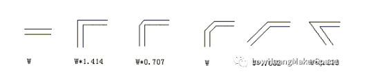
2.2 Trace Geometry and Layer Stackup
- Microstrip impedance is calculated as:
[
Z_0 \approx \frac{87}{\sqrt{\epsilon_r + 1.41}} \ln \left( \frac{5.98H}{0.8W + T} \right)
] - Stripline impedance is given by:
[
Z_0 \approx \frac{60}{\sqrt{\epsilon_r}} \ln \left( \frac{4H}{0.67W (0.8 + T/W)} \right)
]
A well-designed layer stackup ensures controlled impedance by maintaining consistent dielectric spacing.
2.3 Manufacturing Tolerances
Variations in etching (trace width deviations), dielectric thickness, and copper plating affect impedance. Tight manufacturing tolerances (±10% or better) are necessary for high-speed designs.
2.4 Crosstalk and EMI Considerations
Adjacent traces can introduce crosstalk, altering impedance. Proper spacing and shielding techniques (e.g., ground planes, differential pairs) mitigate interference.
3. Techniques for Impedance Control
3.1 Controlled Dielectric Materials
Using prepregs and core materials with precise Dk values ensures consistency. High-frequency laminates (e.g., Rogers 4000 series) offer better performance than standard FR-4.
3.2 Differential Pair Routing
For high-speed interfaces (e.g., USB, PCIe), differential signaling uses two complementary traces with tightly controlled impedance (typically 90Ω or 100Ω differential). Maintaining equal trace lengths minimizes skew.
3.3 Impedance Matching Techniques
- Termination resistors (series or parallel) reduce reflections by matching source/load impedance to the transmission line.
- Stub elimination (via optimization) minimizes impedance discontinuities.
3.4 Simulation and Testing
- Electromagnetic (EM) simulation tools (e.g., Ansys HFSS, CST, or Altium’s field solvers) predict impedance before fabrication.
- Time-Domain Reflectometry (TDR) measures actual impedance post-production.
4. Challenges in Impedance Control
4.1 High-Frequency Signal Loss
At GHz frequencies, skin effect and dielectric loss increase attenuation, requiring low-loss materials and optimized trace geometries.
4.2 Multi-Layer PCB Complexity
Impedance control becomes challenging in dense multi-layer boards due to interactions between adjacent traces and planes.
4.3 Cost vs. Performance Trade-offs
Tighter impedance tolerances increase manufacturing costs. Designers must balance performance requirements with budget constraints.
5. Future Trends in Impedance Control
5.1 Advanced Materials
Emerging substrates (e.g., PTFE-based laminates) offer lower loss and better high-frequency stability.
5.2 3D and Flexible PCBs
Impedance control in flexible PCBs and 3D-printed circuits requires new modeling techniques.
5.3 AI-Driven Design Optimization
Machine learning algorithms can automate impedance tuning, reducing design iteration time.
Conclusion
Characteristic impedance control is a fundamental aspect of high-speed PCB design, ensuring signal integrity and minimizing electromagnetic interference. By carefully selecting materials, optimizing trace geometries, and leveraging simulation tools, engineers can achieve precise impedance matching. As electronic systems continue to push toward higher frequencies, advancements in materials and design methodologies will further enhance impedance control, enabling faster and more reliable PCB performance.