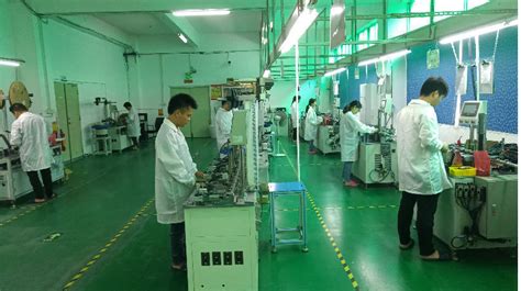
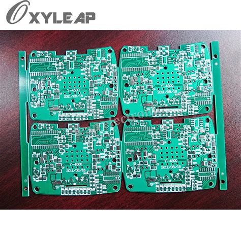
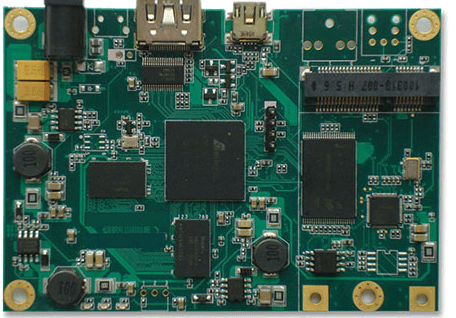
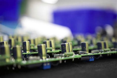
Chemicals used in pcb manufacturing
Understanding the Role of Etching Agents in PCB Manufacturing
In the intricate world of printed circuit board (PCB) manufacturing, the role of etching agents is pivotal. These chemicals are essential in defining the intricate pathways that allow electronic components to communicate effectively. Understanding the role of etching agents in PCB manufacturing requires a closer examination of the processes involved and the specific chemicals used to achieve precision and efficiency.
Initially, the PCB manufacturing process begins with a substrate, typically made of fiberglass or other insulating materials, which is coated with a thin layer of conductive copper.
The objective is to remove unwanted copper to create the desired circuit pattern. This is where etching agents come into play. The etching process involves selectively removing copper from the board, leaving behind the intricate network of conductive paths that form the circuit.
One of the most commonly used etching agents in PCB manufacturing is ferric chloride.
This chemical is favored for its effectiveness in dissolving copper, making it a staple in the industry. Ferric chloride is an acidic solution that reacts with copper to form copper chloride, which is soluble in water. This reaction allows for the precise removal of copper, ensuring that the remaining pathways are clean and well-defined. However, the use of ferric chloride requires careful handling due to its corrosive nature and potential environmental impact.
In addition to ferric chloride, ammonium persulfate is another etching agent frequently employed in PCB manufacturing.
This chemical offers a cleaner etching process, producing fewer residues compared to ferric chloride. Ammonium persulfate is particularly advantageous in applications where high precision is required, as it provides a more controlled etching rate. Despite its benefits, it is essential to manage the concentration and temperature of the ammonium persulfate solution to achieve optimal results.
Moreover, cupric chloride is another etching agent that has gained popularity in recent years.
It is often used in combination with hydrochloric acid to enhance its etching capabilities. Cupric chloride offers the advantage of being regenerable, meaning it can be reused multiple times, which contributes to cost efficiency and environmental sustainability. This characteristic makes it an attractive option for manufacturers seeking to minimize waste and reduce chemical consumption.
Transitioning from the chemical properties to the practical application, the choice of etching agent depends on several factors, including the type of PCB being manufactured, the desired precision, and environmental considerations. Manufacturers must carefully select the appropriate etching agent to balance these factors effectively. Additionally, the etching process must be meticulously controlled to prevent over-etching, which can lead to defects in the circuit pattern and compromise the functionality of the PCB.
Furthermore, advancements in technology have led to the development of alternative etching methods, such as plasma etching and laser etching.
These methods offer increased precision and reduced chemical usage, aligning with the industry’s growing emphasis on sustainability. However, traditional chemical etching remains prevalent due to its cost-effectiveness and established reliability.
In conclusion, etching agents play a crucial role in PCB manufacturing by enabling the precise removal of copper to create intricate circuit patterns. The choice of etching agent, whether it be ferric chloride, ammonium persulfate, or cupric chloride, is influenced by various factors, including precision requirements and environmental impact. As the industry continues to evolve, the integration of new technologies and sustainable practices will further shape the role of etching agents in PCB manufacturing, ensuring that they remain a cornerstone of this essential process.
The Importance of Solder Masks in PCB Production
In the intricate world of printed circuit board (PCB) manufacturing, the role of solder masks is paramount, serving as a critical component that ensures both the functionality and longevity of the final product. Solder masks, often referred to as solder resist, are a thin layer of polymer applied to the copper traces of a PCB. This layer is not merely decorative; it plays a vital role in protecting the board from environmental factors and ensuring the precision of the soldering process. Understanding the importance of solder masks requires a closer examination of their functions and the chemicals involved in their application.
To begin with, solder masks are essential in preventing solder bridges, which occur when solder connects two or more adjacent pads unintentionally.
This can lead to short circuits and ultimately, the failure of the electronic device. By covering the areas of the PCB that should not be soldered, solder masks ensure that solder only adheres to the designated pads. This precision is crucial, especially as electronic devices become more compact and the spacing between components decreases. The application of solder masks thus enhances the reliability and performance of the PCB.
Moreover, solder masks provide a protective barrier against environmental contaminants such as moisture, dust, and chemicals, which can corrode the copper traces and lead to circuit failure.
The polymer layer acts as an insulator, safeguarding the board from potential damage and extending its operational life. This protective quality is particularly important in harsh environments where electronic devices are exposed to extreme conditions. By preventing corrosion and oxidation, solder masks maintain the integrity of the PCB over time.
The application of solder masks involves a series of chemical processes that require precision and expertise.
Typically, the process begins with the cleaning of the PCB surface to remove any contaminants that might interfere with the adhesion of the solder mask. This is followed by the application of a photosensitive epoxy-based ink, which is then exposed to ultraviolet light through a photomask. The areas exposed to the light harden, while the unexposed areas remain soft and are subsequently washed away. This process, known as photolithography, ensures that the solder mask is applied only to the desired areas of the PCB.
The chemicals used in the solder mask process are carefully selected to achieve the desired properties of adhesion, flexibility, and resistance to heat and chemicals.
Epoxy resins are commonly used due to their excellent insulating properties and resistance to environmental factors. Additionally, the use of UV-curable inks allows for precise control over the application process, ensuring that the solder mask adheres only to the intended areas.
In conclusion, solder masks are an indispensable component in PCB manufacturing, providing both functional and protective benefits. By preventing solder bridges and protecting against environmental damage, they enhance the reliability and longevity of electronic devices. The chemical processes involved in their application are complex, requiring careful selection and handling of materials to achieve optimal results. As technology continues to advance and the demand for smaller, more efficient electronic devices grows, the importance of solder masks in PCB production will only continue to increase, underscoring their critical role in the electronics industry.
Exploring the Use of Photoresists in PCB Fabrication
In the intricate world of printed circuit board (PCB) manufacturing, the use of photoresists plays a pivotal role in defining the precision and functionality of the final product. Photoresists are light-sensitive materials that are essential in the photolithography process, a critical step in PCB fabrication. This process involves transferring a circuit pattern onto a substrate, which is typically a copper-clad laminate. The application of photoresists ensures that the intricate designs of electronic circuits are accurately imprinted onto the board, thereby facilitating the creation of complex electronic devices.
To begin with, photoresists are categorized into two main types: positive and negative.
Positive photoresists become soluble when exposed to ultraviolet (UV) light, allowing the exposed areas to be washed away during development. This results in a pattern that matches the mask used during exposure. Conversely, negative photoresists harden upon exposure to UV light, meaning the unexposed areas are removed during development. The choice between positive and negative photoresists depends on various factors, including the desired resolution, the complexity of the circuit design, and the specific requirements of the manufacturing process.
The application of photoresists in PCB fabrication involves several meticulous steps.
Initially, the substrate is thoroughly cleaned to remove any contaminants that could interfere with the adhesion of the photoresist. Following this, a uniform layer of photoresist is applied to the substrate using techniques such as spin coating or spray coating. The coated substrate is then subjected to a soft bake process, which removes solvents and enhances the adhesion of the photoresist to the substrate. This step is crucial in ensuring that the photoresist layer is uniform and free from defects.
Subsequently, the substrate is aligned with a photomask, which contains the desired circuit pattern.
The assembly is then exposed to UV light, which alters the chemical structure of the photoresist in the exposed areas. This exposure step is critical, as it determines the accuracy and resolution of the circuit pattern. After exposure, the substrate undergoes a development process, where a developer solution is used to remove the soluble portions of the photoresist. This step reveals the underlying copper layer in the pattern of the circuit design.
Following development, the substrate is subjected to a hard bake process, which further solidifies the remaining photoresist and enhances its resistance to subsequent chemical processes.
The exposed copper areas are then etched away using chemical etchants, leaving behind the desired circuit pattern protected by the hardened photoresist. Finally, the remaining photoresist is stripped away, revealing the completed circuit pattern on the substrate.
Throughout this process, the choice of photoresist and the precision of each step are paramount in achieving high-quality PCBs. Advances in photoresist technology continue to push the boundaries of what is possible in PCB fabrication, enabling the production of increasingly complex and miniaturized electronic devices. As the demand for more sophisticated electronics grows, the role of photoresists in PCB manufacturing will undoubtedly remain a cornerstone of the industry, driving innovation and ensuring the reliability of electronic components.

Chemical Cleaning Agents: Ensuring PCB Quality and Reliability
In the intricate world of printed circuit board (PCB) manufacturing, the role of chemical cleaning agents is paramount in ensuring the quality and reliability of the final product. As PCBs form the backbone of virtually all electronic devices, their performance and longevity are critical. Therefore, the cleaning process, which involves the removal of contaminants that could potentially compromise the functionality of the circuit board, is a crucial step in the manufacturing process. To achieve this, a variety of chemical cleaning agents are employed, each serving a specific purpose and contributing to the overall integrity of the PCB.
Initially, it is essential to understand the types of contaminants that can affect PCBs.
These include residues from soldering processes, such as flux, as well as dust, oils, and other particulates that may accumulate during manufacturing. If not adequately removed, these contaminants can lead to issues such as poor electrical connectivity, corrosion, and even complete failure of the electronic device. Consequently, the selection of appropriate chemical cleaning agents is vital to mitigate these risks.
One of the most commonly used cleaning agents in PCB manufacturing is isopropyl alcohol (IPA).
Known for its effectiveness in dissolving a wide range of organic and inorganic residues, IPA is favored for its ability to clean without leaving behind any significant residues. Its volatility ensures that it evaporates quickly, reducing the risk of moisture-related issues. However, while IPA is effective for general cleaning, it may not be sufficient for removing more stubborn contaminants, necessitating the use of more specialized agents.
For more challenging cleaning tasks, manufacturers often turn to aqueous cleaning solutions.
These solutions typically consist of water mixed with various surfactants and saponifiers, which work together to break down and remove residues. Aqueous cleaners are particularly effective at removing flux residues, which can be difficult to eliminate with solvents alone. Moreover, they are considered more environmentally friendly compared to some solvent-based cleaners, aligning with the industry’s growing emphasis on sustainability.
In addition to aqueous solutions, semi-aqueous cleaners are also employed in PCB manufacturing.
These cleaners combine the strengths of both solvent and aqueous cleaning methods, using organic solvents to dissolve contaminants and water to rinse them away. This dual-action approach makes semi-aqueous cleaners highly effective for a wide range of residues, offering a balance between cleaning power and environmental considerations.
Furthermore, the use of ultrasonic cleaning technology has become increasingly prevalent in conjunction with chemical cleaning agents
Ultrasonic cleaners use high-frequency sound waves to agitate the cleaning solution, enhancing its ability to penetrate and remove contaminants from even the most intricate PCB designs. This method is particularly beneficial for cleaning complex assemblies where manual cleaning would be impractical or insufficient.
In conclusion, the selection and application of chemical cleaning agents in PCB manufacturing are critical to ensuring the quality and reliability of the final product. By effectively removing contaminants, these agents help prevent potential failures and extend the lifespan of electronic devices. As the industry continues to evolve, the development of new and improved cleaning agents will remain a focal point, driven by the dual imperatives of performance and environmental responsibility. Through the careful integration of these chemical solutions, manufacturers can uphold the high standards required in today’s technologically advanced world.