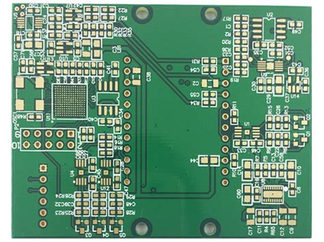
China high speed pcb design
Innovations In High-Speed PCB Design For China’s Tech Industry
In recent years, China’s tech industry has witnessed remarkable advancements, particularly in the realm of high-speed printed circuit board (PCB) design. As the demand for faster and more efficient electronic devices continues to surge, the need for innovative PCB solutions has become increasingly critical.
High-speed PCBs are essential for supporting the rapid data transmission rates required by modern applications, such as 5G telecommunications, advanced computing systems, and cutting-edge consumer electronics. Consequently, Chinese engineers and designers are at the forefront of developing new techniques and technologies to meet these demands.
One of the key innovations in high-speed PCB design is the implementation of advanced materials.
Traditional PCB materials, such as FR-4, are often inadequate for high-frequency applications due to their limited electrical performance. To address this, Chinese manufacturers are increasingly turning to high-performance laminates, such as polytetrafluoroethylene (PTFE) and ceramic-filled substrates, which offer superior dielectric properties and thermal stability. These materials enable the creation of PCBs that can handle higher frequencies and faster signal transmission, thereby enhancing the overall performance of electronic devices.
In addition to material advancements, the miniaturization of components has also played a significant role in the evolution of high-speed PCB design.
As devices become smaller and more compact, the need for densely packed PCBs has grown. Chinese designers are leveraging innovative techniques, such as microvia technology and high-density interconnect (HDI) designs, to maximize the use of available space on a PCB. These approaches allow for more components to be integrated into a smaller area, reducing signal path lengths and minimizing potential interference, which is crucial for maintaining signal integrity at high speeds.
Moreover, the integration of simulation and modeling tools has revolutionized the design process for high-speed PCBs.
Chinese engineers are utilizing sophisticated software to simulate the electrical behavior of PCBs before they are physically manufactured. This allows for the identification and mitigation of potential issues, such as signal reflection and crosstalk, early in the design phase. By optimizing the layout and routing of traces, designers can ensure that the final product meets the stringent performance requirements of high-speed applications.
Furthermore, the rise of artificial intelligence (AI) and machine learning (ML) technologies is beginning to influence high-speed PCB design in China.
These technologies are being used to automate various aspects of the design process, from component placement to trace routing. By analyzing vast amounts of data, AI and ML algorithms can identify patterns and suggest optimal design solutions, significantly reducing the time and effort required to develop complex PCBs. This not only accelerates the design cycle but also enhances the reliability and performance of the final product.
In conclusion, the innovations in high-speed PCB design are playing a pivotal role in propelling China’s tech industry forward.
Through the adoption of advanced materials, miniaturization techniques, simulation tools, and AI-driven design processes, Chinese engineers are overcoming the challenges associated with high-speed applications. As the demand for faster and more efficient electronic devices continues to grow, these innovations will undoubtedly remain at the forefront of technological development, ensuring that China’s tech industry remains competitive on the global stage.
Challenges And Solutions In China’s High-Speed PCB Manufacturing
China’s high-speed PCB (Printed Circuit Board) manufacturing industry has experienced significant growth over the past few decades, driven by the increasing demand for advanced electronic devices and the rapid development of technology. However, this growth has not been without its challenges. The complexity of high-speed PCB design presents numerous obstacles that manufacturers must overcome to maintain their competitive edge in the global market. Understanding these challenges and exploring potential solutions is crucial for the continued success of China’s PCB industry.
One of the primary challenges in high-speed PCB manufacturing is signal integrity.
As electronic devices become more sophisticated, the need for faster data transmission rates increases. This demand necessitates the use of high-speed PCBs, which are designed to handle rapid signal transmission without degradation. However, maintaining signal integrity at high speeds is a complex task. Factors such as impedance mismatches, crosstalk, and electromagnetic interference can significantly affect the performance of a PCB. To address these issues, manufacturers must employ advanced design techniques and tools. For instance, using simulation software to model and predict signal behavior can help identify potential problems before they occur, allowing for adjustments in the design phase.
Another significant challenge is thermal management.
High-speed PCBs often operate at elevated temperatures due to the increased power density and faster switching speeds. Excessive heat can lead to component failure and reduced reliability, making effective thermal management a critical aspect of PCB design. Solutions to this challenge include the use of thermal vias, heat sinks, and advanced materials with high thermal conductivity. Additionally, optimizing the layout to minimize heat generation and improve heat dissipation can enhance the overall performance and longevity of the PCB.
The miniaturization of electronic components also poses a challenge in high-speed PCB manufacturing.
As devices become smaller and more compact, the demand for PCBs with higher component density increases. This trend requires manufacturers to develop innovative solutions to accommodate more components in a limited space without compromising performance. Techniques such as multi-layer PCB design and the use of microvias can help achieve higher component density. Furthermore, advancements in manufacturing processes, such as laser drilling and precision etching, enable the production of PCBs with finer features and tighter tolerances.
Material selection is another critical factor in high-speed PCB design.
The choice of materials can significantly impact the electrical performance, thermal management, and overall reliability of the PCB. High-frequency laminates, for example, are essential for maintaining signal integrity at high speeds. These materials offer low dielectric loss and stable electrical properties, making them suitable for high-speed applications. However, they can be more expensive and challenging to work with compared to traditional materials. Manufacturers must carefully balance performance requirements with cost considerations to select the most appropriate materials for their designs.
In conclusion, while China’s high-speed PCB manufacturing industry faces several challenges, there are numerous solutions available to address these issues. By leveraging advanced design techniques, optimizing thermal management, embracing miniaturization, and selecting appropriate materials, manufacturers can overcome the obstacles associated with high-speed PCB design. As the demand for faster and more efficient electronic devices continues to grow, the ability to navigate these challenges will be crucial for maintaining China’s position as a leader in the global PCB market. Through innovation and adaptation, the industry can continue to thrive and meet the evolving needs of technology-driven markets worldwide.

The Role Of High-Speed PCB Design In China’s 5G Network Expansion
The rapid expansion of 5G networks in China has underscored the critical role of high-speed printed circuit board (PCB) design in supporting this technological advancement. As the demand for faster and more reliable communication networks intensifies, the need for sophisticated PCB designs that can handle high-speed data transmission becomes increasingly apparent. High-speed PCB design is pivotal in ensuring that the infrastructure supporting 5G networks is both efficient and effective, thereby facilitating the seamless integration of this next-generation technology across the nation.
To understand the significance of high-speed PCB design in China’s 5G network expansion, it is essential to consider the technical requirements of 5G technology.
Unlike its predecessors, 5G networks necessitate the transmission of vast amounts of data at unprecedented speeds. This requirement places immense pressure on the underlying hardware, particularly the PCBs, which serve as the backbone of electronic devices. High-speed PCBs are designed to manage these demands by minimizing signal loss and interference, thereby ensuring that data is transmitted quickly and accurately.
In China, the development of high-speed PCB design has been driven by both government initiatives and private sector innovation.
The Chinese government has recognized the strategic importance of 5G technology and has invested heavily in research and development to support its deployment. This investment has spurred advancements in PCB design, as companies strive to create solutions that meet the stringent requirements of 5G networks. Moreover, the competitive nature of the Chinese technology market has fostered a culture of innovation, with numerous firms vying to develop cutting-edge PCB designs that can support high-speed data transmission.
One of the key challenges in high-speed PCB design is managing signal integrity.
As data speeds increase, the risk of signal degradation becomes more pronounced, potentially leading to errors and reduced performance. To address this issue, designers employ a range of techniques, such as impedance matching and the use of advanced materials, to ensure that signals are transmitted with minimal loss. Additionally, the layout of the PCB is meticulously planned to reduce electromagnetic interference, which can further compromise signal integrity.
Another critical aspect of high-speed PCB design is thermal management.
The increased data rates associated with 5G networks generate significant heat, which can adversely affect the performance and longevity of electronic components. Effective thermal management strategies, such as the incorporation of heat sinks and the use of thermally conductive materials, are essential to dissipate heat and maintain optimal operating conditions.
The role of high-speed PCB design in China’s 5G network expansion is not limited to technical considerations.
It also has significant economic implications, as the successful deployment of 5G technology is expected to drive growth across various sectors. By enabling faster and more reliable communication, 5G networks can support the development of smart cities, autonomous vehicles, and the Internet of Things, among other innovations. Consequently, the advancement of high-speed PCB design is integral to realizing the full potential of 5G technology and ensuring that China remains at the forefront of this global technological revolution.
In conclusion, high-speed PCB design is a cornerstone of China’s 5G network expansion, playing a crucial role in meeting the technical demands of this advanced communication technology. Through a combination of government support and private sector innovation, China is poised to lead the way in 5G deployment, with high-speed PCB design serving as a key enabler of this progress. As the nation continues to invest in and develop this critical technology, the impact of high-speed PCB design on China’s technological landscape will undoubtedly be profound and far-reaching.
Future Trends In High-Speed PCB Design In China
As the global demand for advanced electronics continues to surge, China stands at the forefront of high-speed printed circuit board (PCB) design, a critical component in the development of cutting-edge technology. The future of high-speed PCB design in China is poised for significant evolution, driven by technological advancements, increased investment in research and development, and the growing need for faster, more efficient electronic devices. Understanding these future trends is essential for stakeholders in the electronics industry, as they navigate the complexities of this rapidly changing landscape.
One of the most prominent trends in high-speed PCB design in China is the integration of artificial intelligence (AI) and machine learning (ML) technologies.
These technologies are being increasingly utilized to optimize the design process, allowing for more precise and efficient PCB layouts. By leveraging AI and ML, designers can predict potential issues and optimize signal integrity, thereby reducing the time and cost associated with traditional trial-and-error methods. This shift towards intelligent design processes is expected to enhance the overall quality and performance of high-speed PCBs, making them more reliable and efficient.
Moreover, the miniaturization of electronic components continues to be a driving force in the evolution of high-speed PCB design.
As devices become smaller and more compact, the demand for PCBs that can accommodate these changes without compromising performance is growing. In response, Chinese manufacturers are investing in advanced materials and innovative design techniques that allow for higher component density and improved thermal management. This trend towards miniaturization not only supports the development of smaller devices but also contributes to the overall sustainability of electronic products by reducing material usage and energy consumption.
In addition to technological advancements, the future of high-speed PCB design in China is also being shaped by the country’s strategic focus on developing its semiconductor industry.
The Chinese government has been actively promoting policies and initiatives aimed at boosting domestic semiconductor production, which in turn influences the PCB industry. As China seeks to reduce its reliance on foreign technology, there is a concerted effort to enhance local capabilities in high-speed PCB design and manufacturing. This focus on self-sufficiency is expected to drive innovation and foster a more competitive environment, ultimately benefiting the global electronics market.
Furthermore, the rise of 5G technology is another significant factor influencing the future of high-speed PCB design in China.
The deployment of 5G networks requires PCBs that can handle higher frequencies and faster data transmission rates. As a result, Chinese designers are exploring new materials and design methodologies to meet these demands. The development of PCBs that can support 5G technology is crucial for enabling the next generation of wireless communication devices, and China is well-positioned to lead this charge.
In conclusion, the future trends in high-speed PCB design in China are characterized by a convergence of technological innovation, strategic policy initiatives, and market demands. The integration of AI and ML, the push towards miniaturization, the focus on semiconductor self-sufficiency, and the advent of 5G technology are all shaping the trajectory of this dynamic industry. As China continues to invest in and develop its high-speed PCB capabilities, it is likely to remain a key player in the global electronics landscape, driving advancements that will impact a wide range of industries and applications.