Chip on PCB: Integration, Challenges, and Future Trends
Introduction
The integration of chips onto Printed Circuit Boards (PCBs) is a cornerstone of modern electronics. As devices become smaller, faster, and more complex, the need for efficient and reliable chip-on-PCB integration has grown exponentially. This article explores the fundamentals of chip-on-PCB technology, its applications, challenges, and future trends.
1. Fundamentals of Chip-on-PCB Technology
1.1 What is a Chip on PCB?
A chip, also known as an integrated circuit (IC), is a semiconductor device that contains multiple electronic components such as transistors, resistors, and capacitors. These components are interconnected to perform specific functions, such as processing data, amplifying signals, or storing information. A PCB, on the other hand, is a flat board made of insulating material (typically fiberglass) with conductive pathways etched or printed onto its surface. These pathways, known as traces, connect various electronic components mounted on the board.
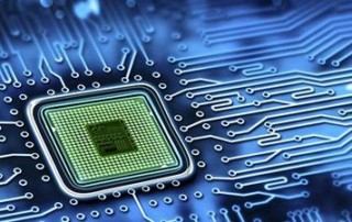
Chip-on-PCB refers to the process of mounting and connecting semiconductor chips directly onto a PCB. This integration allows for the creation of compact, high-performance electronic systems.
1.2 Types of Chip-on-PCB Integration
There are several methods for integrating chips onto PCBs, each with its own advantages and limitations:
- Wire Bonding: This is one of the most common methods, where thin wires are used to connect the chip’s bonding pads to the PCB’s traces. Wire bonding is cost-effective and widely used in low-to-medium complexity applications.
- Flip-Chip Technology: In this method, the chip is flipped upside down and directly soldered onto the PCB using solder bumps. Flip-chip technology offers better electrical performance and thermal management compared to wire bonding, making it suitable for high-speed and high-power applications.
- Chip-on-Board (COB): In COB, the chip is directly mounted onto the PCB and encapsulated with a protective material. This method is often used in applications where space is at a premium, such as in mobile devices.
- Embedded Chip Technology: This advanced method involves embedding the chip within the layers of the PCB itself. Embedded chip technology offers the highest level of integration and is used in applications requiring extreme miniaturization and performance.
2. Applications of Chip-on-PCB Technology
2.1 Consumer Electronics
Chip-on-PCB technology is ubiquitous in consumer electronics, including smartphones, tablets, laptops, and wearable devices. The demand for smaller, lighter, and more powerful devices has driven the adoption of advanced chip-on-PCB integration techniques. For example, flip-chip technology is commonly used in smartphones to connect the processor and memory chips to the PCB, enabling high-speed data processing and compact form factors.
2.2 Automotive Electronics
The automotive industry has seen a significant increase in the use of chip-on-PCB technology, particularly with the rise of electric vehicles (EVs) and advanced driver-assistance systems (ADAS). In EVs, power electronics modules, which control the flow of electricity between the battery and the motor, rely on chip-on-PCB integration for efficient thermal management and high power density. Similarly, ADAS systems, which include features like adaptive cruise control and lane-keeping assist, require high-performance chips to process large amounts of sensor data in real-time.
2.3 Industrial and IoT Applications
In industrial settings, chip-on-PCB technology is used in a wide range of applications, from factory automation to robotics. The Internet of Things (IoT) has further expanded the use of chip-on-PCB integration, as IoT devices often require compact, low-power, and high-performance electronics. For example, smart sensors used in industrial IoT applications often use chip-on-board (COB) technology to achieve the necessary level of integration and reliability.
2.4 Medical Devices
Medical devices, particularly implantable and wearable devices, benefit greatly from chip-on-PCB technology. Implantable devices, such as pacemakers and neurostimulators, require extremely compact and reliable electronics. Chip-on-PCB integration allows these devices to be miniaturized while maintaining high performance and reliability. Wearable medical devices, such as glucose monitors and fitness trackers, also rely on chip-on-PCB technology to achieve small form factors and low power consumption.
3. Challenges in Chip-on-PCB Integration
3.1 Thermal Management
One of the primary challenges in chip-on-PCB integration is managing the heat generated by the chips. As chips become more powerful, they generate more heat, which can lead to performance degradation and even failure if not properly managed. Effective thermal management is particularly critical in high-power applications, such as automotive electronics and data centers.
Several techniques are used to manage heat in chip-on-PCB systems, including:
- Thermal Vias: These are small holes drilled into the PCB and filled with conductive material to help dissipate heat from the chip to other layers of the board or to a heatsink.
- Heat Spreaders: These are metal plates attached to the chip or PCB to spread heat over a larger area, improving heat dissipation.
- Liquid Cooling: In some high-performance applications, liquid cooling systems are used to remove heat from the chip and PCB.
3.2 Signal Integrity
As data rates increase, maintaining signal integrity becomes more challenging. High-speed signals can be affected by issues such as crosstalk, reflection, and attenuation, which can degrade the performance of the system. To address these challenges, designers must carefully consider the layout of the PCB, including the placement of traces, vias, and components.
Techniques to improve signal integrity include:
- Impedance Matching: Ensuring that the impedance of the traces matches the impedance of the chips and other components to minimize signal reflection.
- Differential Signaling: Using pairs of traces to carry complementary signals, which helps to reduce noise and improve signal integrity.
- Shielding: Adding grounded metal layers or shields to protect sensitive signals from interference.
3.3 Mechanical Stress
Chips and PCBs are subject to mechanical stress during manufacturing, assembly, and operation. This stress can lead to issues such as solder joint fatigue, cracking, and delamination, which can affect the reliability of the system. To mitigate these issues, designers must consider factors such as the coefficient of thermal expansion (CTE) mismatch between the chip and PCB, as well as the mechanical properties of the materials used.
Techniques to reduce mechanical stress include:
- Underfill: A material applied between the chip and PCB to provide additional mechanical support and reduce stress on the solder joints.
- Flexible PCBs: In some applications, flexible PCBs are used to reduce mechanical stress and improve reliability.
- Design for Manufacturability (DFM): Designing the PCB and chip layout to minimize stress during assembly and operation.
3.4 Cost and Complexity
As chip-on-PCB technology advances, the cost and complexity of design, manufacturing, and testing increase. Advanced integration techniques, such as flip-chip and embedded chip technology, require specialized equipment and processes, which can drive up costs. Additionally, the complexity of high-density interconnects (HDI) and multi-layer PCBs can make design and testing more challenging.
To address these challenges, manufacturers are investing in advanced manufacturing technologies, such as automated assembly and testing, as well as design tools that can simulate and optimize chip-on-PCB systems.
4. Future Trends in Chip-on-PCB Technology
4.1 Advanced Packaging Technologies
The future of chip-on-PCB technology is closely tied to advancements in packaging technologies. As chips become more complex and powerful, traditional packaging methods may not be sufficient to meet the demands of next-generation electronics. Advanced packaging technologies, such as 2.5D and 3D packaging, are emerging as key enablers of future chip-on-PCB integration.
- 2.5D Packaging: In 2.5D packaging, chips are mounted on an interposer, which is then connected to the PCB. This allows for higher interconnect density and better thermal management compared to traditional packaging methods.
- 3D Packaging: In 3D packaging, multiple chips are stacked vertically and connected using through-silicon vias (TSVs). This approach offers the highest level of integration and performance, making it suitable for applications such as high-performance computing and artificial intelligence.
4.2 Heterogeneous Integration
Heterogeneous integration refers to the integration of different types of chips, such as processors, memory, and sensors, onto a single PCB. This approach allows for the creation of highly optimized systems that can meet the specific requirements of a given application. For example, in autonomous vehicles, heterogeneous integration can be used to combine high-performance processors with specialized sensors and memory chips to create a highly efficient and compact system.
4.3 Flexible and Stretchable Electronics
As the demand for wearable and implantable devices grows, there is increasing interest in flexible and stretchable electronics. These devices require chip-on-PCB integration techniques that can accommodate bending, stretching, and other mechanical deformations. Researchers are exploring new materials and manufacturing processes, such as flexible substrates and stretchable interconnects, to enable the development of next-generation flexible and stretchable electronics.
4.4 AI and Machine Learning in Design and Testing
Artificial intelligence (AI) and machine learning (ML) are increasingly being used to optimize chip-on-PCB design and testing. AI-driven design tools can analyze vast amounts of data to identify optimal layouts, materials, and manufacturing processes. Similarly, ML algorithms can be used to improve the accuracy and efficiency of testing, reducing the time and cost associated with bringing new products to market.
Conclusion
Chip-on-PCB technology is a critical enabler of modern electronics, allowing for the creation of compact, high-performance systems across a wide range of applications. While there are challenges associated with thermal management, signal integrity, mechanical stress, and cost, ongoing advancements in packaging, materials, and design tools are driving the continued evolution of this technology. As we look to the future, trends such as advanced packaging, heterogeneous integration, flexible electronics, and AI-driven design are poised to further revolutionize chip-on-PCB integration, enabling the development of next-generation electronic systems.