Circuit Manufacturing Companies: Driving Next-Gen Tech Innovations
Key Takeaways
When exploring PCB manufacturing advancements, you’ll find that PCB manufacturing companies play a pivotal role in shaping modern technology. These firms enable rapid innovation by balancing PCB manufacturing cost efficiency with precision engineering, ensuring scalable solutions for industries like AI, IoT, and renewable energy.
“Optimizing production workflows is critical for maintaining competitive margins in the PCB manufacturing business,” notes a leading industry analyst.
Here’s a breakdown of how key factors intersect:
| Factor | Impact |
|---|---|
| Advanced Fabrication | Enables complex designs for high-density circuits |
| Cost-Effective Scaling | Reduces PCB manufacturing cost for mass production |
| Rapid Prototyping | Accelerates development cycles by 30-50% |
| Sustainability Practices | Lowers waste in PCB manufacturing by 25% through material innovation |
Modern PCB manufacturing companies leverage modular design principles to adapt to evolving tech demands, such as flexible circuits for wearables or energy-efficient layouts for solar systems. While upfront investments in specialized equipment can raise PCB manufacturing business expenses, long-term savings emerge through automated quality control and optimized material usage.
To stay competitive, prioritize partners offering end-to-end scalability—from prototyping to global distribution. This ensures your projects align with both technical benchmarks and budgetary constraints.
Circuit Manufacturing Powers AI and IoT Growth
Modern advancements in PCB manufacturing are directly fueling breakthroughs in artificial intelligence (AI) and the Internet of Things (IoT). As these technologies demand increasingly compact, high-performance circuitry, PCB manufacturing companies are innovating to deliver precision-engineered solutions. By optimizing PCB manufacturing cost through automated processes and material efficiencies, these firms enable scalable production of multi-layered boards capable of handling AI’s massive data throughput and IoT’s low-power connectivity needs.
Advanced fabrication techniques, such as high-density interconnect (https://www.andwinpcba.com) now offer rapid iteration cycles, ensuring startups and enterprises alike can test and refine designs without prohibitive delays.
As AI algorithms grow more complex and IoT networks expand, the role of PCB manufacturing in bridging hardware capabilities with software demands becomes irreplaceable. Whether you’re developing edge computing modules or smart grid controllers, the precision and scalability of modern circuit fabrication underpin every leap forward.
Advanced PCB Fabrication Techniques Explained
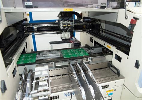
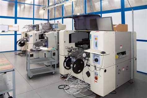
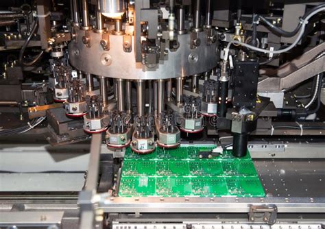
Modern PCB manufacturing relies on precision engineering to meet the demands of today’s high-performance devices. PCB manufacturing companies now employ techniques like high-density interconnect (HDI) and laser direct imaging (LDI) to create circuits with finer traces and tighter tolerances. These advancements reduce PCB manufacturing cost by minimizing material waste and improving yield rates, while enabling complex designs for AI processors and IoT sensors.
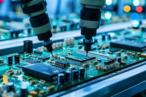
Automated optical inspection (AOI) systems ensure defects are caught early, maintaining quality without slowing production—a critical factor for PCB manufacturing business scalability. Techniques such as embedded component fabrication integrate passive components directly into the board, saving space and enhancing reliability in wearables and medical devices.
You’ll also find innovations like flexible PCBs reshaping industries, from foldable smartphones to aerospace systems. By combining rigid and flexible layers, manufacturers deliver lightweight, durable solutions that endure extreme conditions. These methods not only accelerate prototyping but also align with global sustainability goals through energy-efficient processes.
As demands grow for faster, smaller, and smarter electronics, mastering these techniques ensures PCB manufacturing companies stay ahead in a competitive market—balancing technical excellence with cost-effective scalability.
Rapid Prototyping Accelerates Tech Innovation
When developing cutting-edge technologies, speed often determines market success. PCB manufacturing companies leverage rapid prototyping to compress design cycles, allowing you to test and refine concepts faster than traditional methods. By integrating advanced tools like 3D printing and automated optical inspection, these firms slash PCB manufacturing costs while maintaining precision—critical for AI-driven devices or IoT sensors requiring flawless performance.
This approach isn’t just about speed; it’s about scalability. Prototypes created through streamlined PCB manufacturing processes enable quick validation of complex designs, reducing risks before mass production. For startups or enterprises alike, the ability to iterate designs in days—not weeks—gives a critical competitive edge. Imagine developing a smart wearable: rapid prototyping lets you troubleshoot signal integrity issues early, ensuring your final product meets stringent performance benchmarks.
Moreover, the PCB manufacturing business now prioritizes flexibility. Hybrid models combine rapid prototyping with on-demand production, letting you scale globally without overcommitting resources. Whether you’re building renewable energy controllers or medical IoT devices, this agility ensures your innovations stay ahead of evolving tech demands.
Sustainable Circuit Solutions for Renewable Energy
As renewable energy systems demand higher efficiency and durability, PCB manufacturing companies are pioneering eco-conscious designs that align with global sustainability goals. By integrating recyclable materials like halogen-free substrates and lead-free finishes, modern PCB manufacturing processes minimize environmental impact without compromising performance. You’ll find that advanced techniques such as laser direct imaging and precision etching reduce material waste, directly lowering PCB manufacturing cost while maintaining tight tolerances for solar inverters, wind turbine controllers, and energy storage systems.
For businesses scaling renewable projects, partnering with PCB manufacturing business experts ensures access to green certifications (like UL ECOLOGO or RoHS) and streamlined workflows for complex multilayer boards. Innovations such as embedded passive components further shrink energy losses, critical for maximizing the lifespan of renewable installations. Transitioning to these sustainable methods doesn’t just support environmental stewardship—it future-proofs your supply chain against tightening regulations and shifting market expectations. By prioritizing energy-efficient designs, you enable smarter integration of renewables into grids, creating a ripple effect across the entire clean tech ecosystem.
Global Scalability in Electronics Manufacturing
When scaling electronics production across continents, pcb manufacturing companies play a pivotal role in balancing technical precision with cost-efficiency. By leveraging distributed manufacturing networks, these firms optimize pcb manufacturing cost structures while meeting regional demand spikes—critical for industries like AI or IoT that require rapid deployment. Advanced logistics and modular design frameworks allow seamless adaptation to local regulations, supply chain dynamics, and environmental standards, ensuring consistent quality without compromising speed.
For businesses expanding globally, partnering with pcb manufacturing specialists simplifies navigating complexities like material sourcing, certification processes, and multi-region compliance. This scalability isn’t just about geographic reach—it’s about integrating flexible production models that align with evolving tech demands. Whether supporting renewable energy grids or smart devices, the pcb manufacturing business thrives by merging high-volume capabilities with niche customization, enabling clients to innovate faster while maintaining cost control. The result? A globally interconnected ecosystem where cutting-edge electronics reach markets at unprecedented speed.
Flex Circuits Revolutionizing Device Design
As modern electronics demand thinner, lighter, and more durable designs, flex circuits are reshaping how engineers approach device architecture. Unlike traditional rigid PCB manufacturing, flexible printed circuits eliminate spatial constraints, enabling dynamic form factors for wearables, foldable displays, and implantable medical devices. Leading PCB manufacturing companies now integrate hybrid rigid-flex solutions, merging the reliability of conventional boards with the adaptability of bendable substrates. This shift isn’t just about miniaturization—it’s about reimagining functionality.
When optimizing PCB manufacturing cost, flex circuits offer hidden advantages. Their reduced material waste and simplified assembly processes lower production overheads, while their durability cuts long-term maintenance expenses. For startups in the PCB manufacturing business, this opens doors to scalable, high-mix production without compromising quality. Advanced laser etching and automated alignment systems further ensure precision, even for circuits with micron-level traces.
The rise of IoT and AI-driven devices amplifies the need for flex circuits that withstand extreme conditions—think curved sensors in smart agriculture or vibration-resistant modules in autonomous vehicles. As PCB manufacturing evolves, expect tighter integration between design software and fabrication workflows, accelerating prototyping cycles. Whether you’re developing medical wearables or aerospace systems, flex circuits aren’t just an option—they’re becoming the backbone of next-generation innovation.
Energy Storage Systems and Circuit Innovations
As sustainable energy demands grow, PCB manufacturing companies are developing specialized circuits to optimize energy density and thermal management in storage systems. Modern battery management systems (BMS) rely on high-precision PCB manufacturing techniques to handle fluctuating voltages and ensure efficient power distribution. For instance, layered PCB designs enable compact layouts for lithium-ion battery arrays, while advanced materials like ceramic substrates improve heat dissipation—critical for prolonging battery life.
Balancing PCB manufacturing cost with performance remains a challenge. While thicker copper layers enhance current-carrying capacity for grid-scale storage, they increase material expenses. However, innovations in automated assembly processes help offset these costs, allowing PCB manufacturing businesses to deliver scalable solutions for residential solar setups and industrial microgrids alike.
You’ll also find flexible circuits playing a role in next-gen storage units, adapting to irregular shapes in modular battery packs. These designs not only reduce spatial constraints but also minimize energy loss through shorter conductive pathways. As renewable systems integrate smarter monitoring, PCB manufacturing must support embedded sensors and IoT connectivity—pushing companies to refine multilayer board fabrication for seamless data transmission.
By addressing these technical hurdles, circuit innovators are bridging the gap between renewable energy generation and reliable storage, ensuring your systems operate at peak efficiency across diverse environments.
Next-Gen Prototyping for Smart Technology Demands
Meeting the accelerating demands of smart technology requires PCB manufacturing companies to rethink traditional approaches. Modern prototyping now integrates AI-driven design validation and automated testing, enabling faster iteration cycles for IoT devices, wearables, and autonomous systems. By leveraging advanced PCB fabrication techniques like high-density interconnect (HDI) and embedded component substrates, you can achieve unprecedented precision while reducing PCB manufacturing cost through material optimization.
The shift toward modular prototyping allows businesses to test multiple configurations simultaneously, slashing development timelines by up to 40%. For startups and enterprises alike, partnering with scalable PCB manufacturing businesses ensures access to flexible production capacities, critical for adapting to evolving market needs. Real-time collaboration tools further bridge gaps between design teams and manufacturers, ensuring seamless transitions from concept to mass production.
As smart technologies demand smaller, more energy-efficient circuits, innovations like 3D-printed PCBs and hybrid rigid-flex designs are becoming industry standards. These advancements not only address thermal management challenges but also enhance durability for harsh environments. By prioritizing agile prototyping workflows, you position your projects at the forefront of tech evolution, ready to scale globally without compromising quality or speed.
Conclusion
As you navigate the evolving landscape of modern electronics, PCB manufacturing companies remain indispensable partners in transforming visionary concepts into functional realities. Their expertise in balancing PCB manufacturing cost with precision engineering ensures that innovations—from AI-driven devices to renewable energy grids—are both economically viable and technically robust. By leveraging advanced fabrication techniques, these businesses enable rapid iteration of designs while maintaining strict quality standards, directly supporting your ability to scale solutions globally.
The strategic shift toward sustainable practices in PCB manufacturing not only reduces environmental footprints but also aligns with the growing demand for eco-conscious tech ecosystems. Whether you’re optimizing energy storage systems or prototyping smart devices, partnering with agile PCB manufacturing businesses provides access to cutting-edge materials and processes that accelerate development cycles. As industries push toward smaller, faster, and more interconnected technologies, the role of these specialized manufacturers will only deepen—ensuring your innovations stay ahead in an increasingly competitive market.
FAQs
How do pcb manufacturing companies ensure quality in high-volume production?
Leading pcb manufacturing providers implement automated optical inspection (AOI) and rigorous testing protocols to maintain precision across millions of units. Advanced techniques like laser drilling and multilayer stacking enable consistency, even for complex designs in AI or IoT applications.
What factors influence pcb manufacturing cost for startups?
Costs depend on board complexity, material choices (like high-frequency substrates), and order volume. Many pcb manufacturing businesses offer tiered pricing models, allowing startups to scale production while balancing speed and affordability for rapid prototyping needs.
Can pcb manufacturing support custom designs for renewable energy systems?
Absolutely. Specialized pcb manufacturing companies develop flexible circuits optimized for solar inverters or battery management systems, using heat-resistant materials and sustainable processes to align with green energy goals.
How do you choose between local and global pcb manufacturing partners?
While local suppliers reduce shipping delays, global pcb manufacturing firms often provide broader technical expertise and cost efficiencies. Evaluate their certifications, lead times, and ability to handle mixed-signal designs critical for smart devices.
Ready to Elevate Your Tech Project?
Please click here to explore tailored pcb manufacturing solutions at https://www.andwinpcb.com/pcb-manufacturing/. From prototyping to mass production, discover how optimized workflows can accelerate your innovation timeline.


