Common Issues in Reflow Soldering Process: Causes and Solutions
Introduction
Reflow soldering is a critical process in surface mount technology (SMT) assembly where solder paste is used to attach components to printed circuit boards (PCBs). While reflow soldering offers numerous advantages including high efficiency, consistency, and suitability for mass production, the process is susceptible to various issues that can affect product quality and reliability. This 2000-word article examines the most common problems encountered in reflow soldering, analyzes their root causes, and provides practical solutions to address these challenges.
1. Solder Bridging
Description: Solder bridging occurs when two or more adjacent pads or leads become unintentionally connected by solder, creating short circuits.
Causes:
- Excessive solder paste deposition due to incorrect stencil design or improper printing parameters
- Component misalignment during placement
- Improper reflow profile causing excessive solder flow
- Pad design with insufficient spacing between components
- Solder paste with inappropriate metal content or flux properties
Solutions:
- Optimize stencil design with proper aperture dimensions and thickness (typically 1:1 or 0.66:1 area ratio)
- Implement precise solder paste printing with proper squeegee pressure and speed
- Ensure accurate component placement with vision systems
- Adjust reflow profile to achieve proper wetting without excessive flow
- Use solder paste with appropriate viscosity and metal content (typically 88-90% for standard applications)
- Consider narrower pad designs or solder mask dams between pads for fine-pitch components
2. Tombstoning (Component Lifting)
Description: Tombstoning refers to the condition where one end of a surface mount component lifts from the PCB pad during reflow, standing vertically like a tombstone.
Causes:
- Uneven heating of component terminals
- Imbalanced pad sizes or thermal masses
- Incorrect component placement alignment
- Excessive paste volume on one pad
- Different wetting rates between component terminations and PCB pads
Solutions:
- Design symmetrical pads with equal size and thermal characteristics
- Ensure uniform solder paste deposition on both pads
- Optimize reflow profile to achieve even heating across all components
- Use components with balanced termination metallization
- Consider slower ramp rates during preheat to minimize thermal gradients
- Implement proper pad spacing (typically 0.1-0.2mm larger than component for chip components)
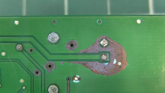
3. Voiding in Solder Joints
Description: Voids are gas pockets trapped within solder joints that can compromise mechanical strength and thermal conductivity.
Causes:
- Outgassing from flux or solder paste during reflow
- Contamination on pads or components
- Improper reflow profile (especially ramp rate)
- Moisture absorption in solder paste or components
- Insufficient time in the liquidous phase
Solutions:
- Optimize reflow profile with proper soak and peak temperatures
- Ensure adequate time above liquidus (typically 60-90 seconds)
- Use solder paste with low voiding characteristics
- Implement proper storage and handling of solder paste (typically refrigerated at 0-10°C)
- Pre-bake moisture-sensitive components when necessary
- Improve pad design for better gas escape (thermal relief patterns)
- Consider vacuum reflow for critical applications
4. Cold Solder Joints
Description: Cold joints appear dull, grainy, and poorly wetted, resulting in weak mechanical and electrical connections.
Causes:
- Insufficient peak temperature during reflow
- Inadequate time above solder liquidus
- Contaminated pads or component terminations
- Excessive cooling rates
- Oxidation of solderable surfaces
- Incorrect solder alloy composition
Solutions:
- Verify and adjust reflow profile to achieve proper peak temperature (typically 20-40°C above solder liquidus)
- Ensure adequate time above liquidus temperature
- Implement proper PCB and component storage to prevent oxidation
- Use nitrogen atmosphere in reflow oven when necessary
- Verify solder paste specifications and storage conditions
- Consider solderability testing for PCBs and components
- Implement proper cleaning processes when required
5. Solder Balling
Description: Small spheres of solder separate from the main joint and scatter across the PCB surface.
Causes:
- Rapid heating causing solder paste splattering
- Excessive solder paste volume
- Poor quality or expired solder paste
- Incorrect reflow atmosphere (oxidation)
- Moisture in solder paste or PCB
- Insufficient flux activity
Solutions:
- Optimize preheat stage of reflow profile (typically 1-2°C/second ramp rate)
- Use fresh solder paste within recommended shelf life
- Implement proper stencil cleaning to prevent paste buildup
- Ensure adequate drying of PCBs before assembly
- Consider solder paste with appropriate flux activity
- Adjust solder paste deposition volume
- Implement proper humidity control in production environment (typically 30-60% RH)
6. Component Damage
Description: Thermal or mechanical damage to components during reflow process.
Causes:
- Excessive peak temperatures
- Too rapid temperature changes (thermal shock)
- Prolonged time at high temperatures
- Incompatible component materials with reflow profile
- Mechanical stress during handling
Solutions:
- Develop component-specific reflow profiles for sensitive parts
- Implement graduated thermal profiles for mixed-technology boards
- Follow manufacturer’s recommendations for temperature-sensitive components
- Consider two-stage reflow for boards with large thermal mass variations
- Use proper handling procedures to prevent mechanical stress
- Implement thermal verification for all components on PCB
7. Insufficient or Excessive Solder
Description: Joints with either inadequate solder volume or excessive solder that may affect reliability.
Causes:
- Incorrect stencil thickness or aperture design
- Improper solder paste printing parameters
- Solder paste slump before reflow
- Uneven PCB surface or warpage
- Squeegee wear or improper pressure
Solutions:
- Optimize stencil design for each component type
- Implement regular stencil cleaning and inspection
- Use appropriate solder paste viscosity for application
- Verify PCB flatness and support during printing
- Monitor and replace squeegees as needed (typically after 50,000-100,000 prints)
- Implement solder paste inspection (SPI) systems for process control
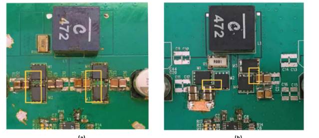
8. Head-in-Pillow Defects
Description: A condition where the component termination and PCB pad are both properly wetted with solder but fail to merge into a complete joint.
Causes:
- Component warpage during reflow
- Oxidation of surfaces
- Insufficient reflow temperature or time
- Poor solder paste quality
- Incompatible materials
Solutions:
- Implement proper component storage to prevent oxidation
- Use solder paste with active flux formulations
- Optimize reflow profile for complete coalescence
- Consider components with better coplanarity specifications
- Use nitrogen atmosphere in reflow oven when necessary
- Implement pre-reflow baking for moisture-sensitive components
9. Flux Residue Issues
Description: Excessive or corrosive flux residue remaining after reflow that may cause electrical or cosmetic problems.
Causes:
- Incomplete flux activation or burnout
- Low-quality flux formulations
- Insufficient peak temperature
- No-clean flux not properly processed
- Incompatible flux chemistry with application
Solutions:
- Optimize reflow profile for complete flux burnout
- Select appropriate flux type for application (RA, RMA, or no-clean)
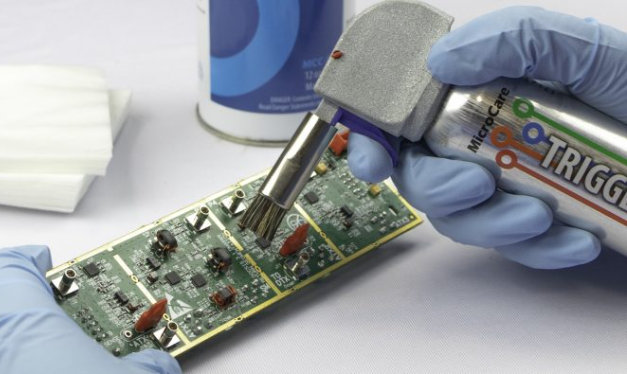
- Implement post-reflow cleaning when required
- Verify compatibility of flux residues with product requirements
- Consider conformal coating for sensitive applications
- Conduct ionic contamination testing when reliability is critical
Process Optimization and Prevention Strategies
To minimize reflow soldering issues, implement these comprehensive strategies:
- Design for Manufacturing (DFM):
- Collaborate with PCB designers to optimize pad layouts
- Consider thermal mass distribution across the board
- Standardize component footprints where possible
- Process Control:
- Implement Statistical Process Control (SPC) for critical parameters
- Regular maintenance and calibration of equipment
- Documented procedures for all process steps
- Material Management:
- Proper storage and handling of solder paste
- First-in-first-out (FIFO) inventory control
- Moisture-sensitive component handling protocols
- Training and Documentation:
- Comprehensive operator training programs
- Clear work instructions and process documentation
- Troubleshooting guides for common issues
- Inspection and Testing:
- Automated Optical Inspection (AOI) systems
- X-ray inspection for hidden joints and voids
- Regular solderability testing
Conclusion
Reflow soldering is a complex process influenced by numerous factors including material properties, equipment parameters, and environmental conditions. By understanding the common issues, their root causes, and implementing appropriate solutions, manufacturers can significantly improve product quality and yield. Continuous process monitoring, regular equipment maintenance, and operator training are essential for maintaining consistent reflow soldering results. As component sizes continue to shrink and lead-free requirements evolve, staying informed about best practices in reflow soldering becomes increasingly critical for electronics manufacturing success.
The key to successful reflow soldering lies in a systematic approach that addresses all aspects of the process – from initial PCB design to final inspection. By applying the solutions outlined in this article and maintaining rigorous process controls, manufacturers can minimize defects and produce reliable electronic assemblies that meet today’s demanding quality standards.